
Multi-bit-per-cell nvm structures and architecture

a multi-bit, cell technology, applied in the direction of digital storage, semiconductor devices, instruments, etc., can solve the problems of reducing electrostatic integrity, reducing scalability, and difficult scaling of current si floating-gate memory devices to gate lengths below 50 nm, so as to reduce sensitivity to charge, and mitigate against readability variation

Inactive Publication Date: 2007-07-19
RGT UNIV OF CALIFORNIA
View PDF5 Cites 241 Cited by
  • Summary
  • Abstract
  • Description
  • Claims
  • Application Information

AI Technical Summary

Benefits of technology

This patent describes a way to create non-volatile memory cells that can store multiple bits of information without being affected by other bits. The invention involves modifying a transistor structure to include a charge-trapping region that is sensitive to changes in the current density. The transistor structure can be a single-gate or double-gate structure, and can include a thin-body or thick-body structure. The invention also describes a novel read method that is sensitive to charge stored in the bit next to the drain electrode. Overall, the invention provides a way to create highly reliable and efficient non-volatile memory cells.

Problems solved by technology

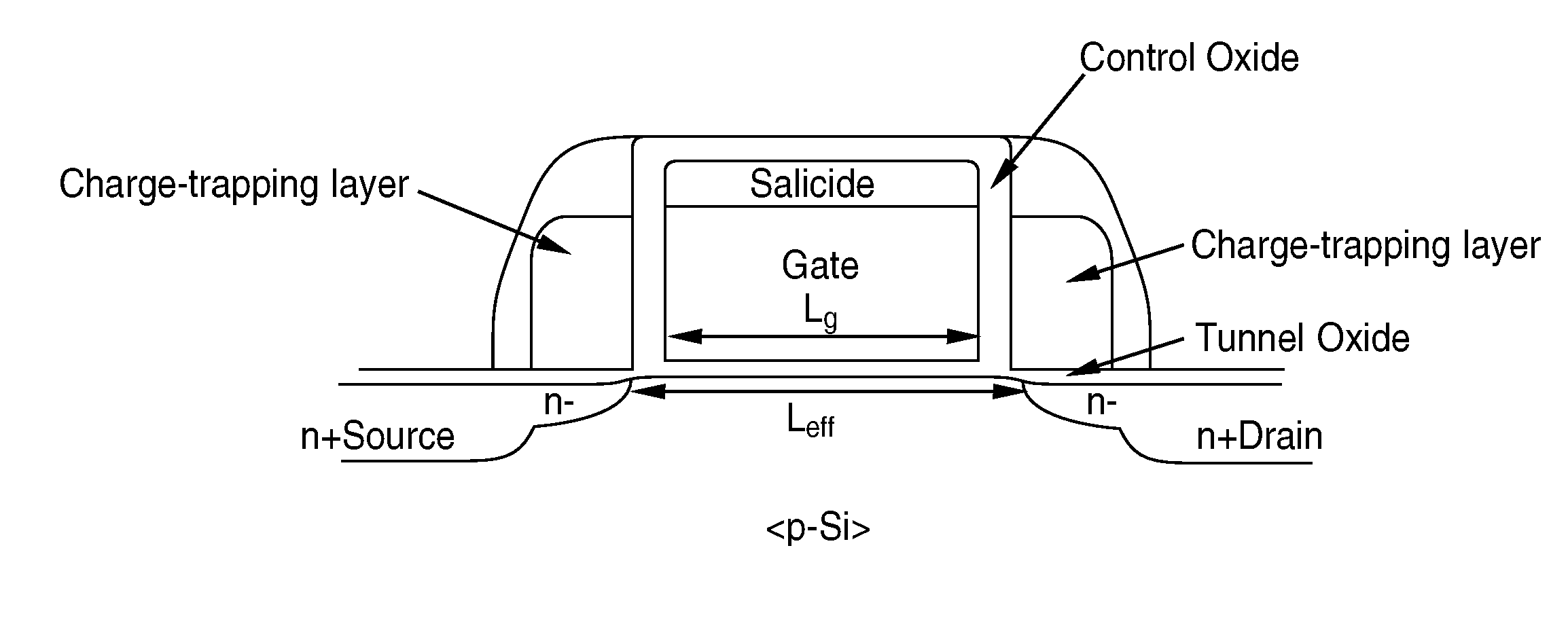
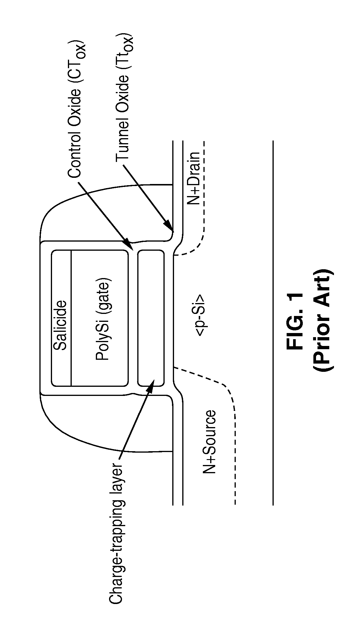
However, current Si floating-gate memory devices are difficult to scale to gate lengths below 50 nm because of their large gate-stack equivalent oxide thickness (EOT).
Still, a conventional SONOS memory device requires a substantially thicker EOT (˜10 nm) than a logic device (˜2 nm) thereby reducing electrostatic integrity, wherein scalability declines.
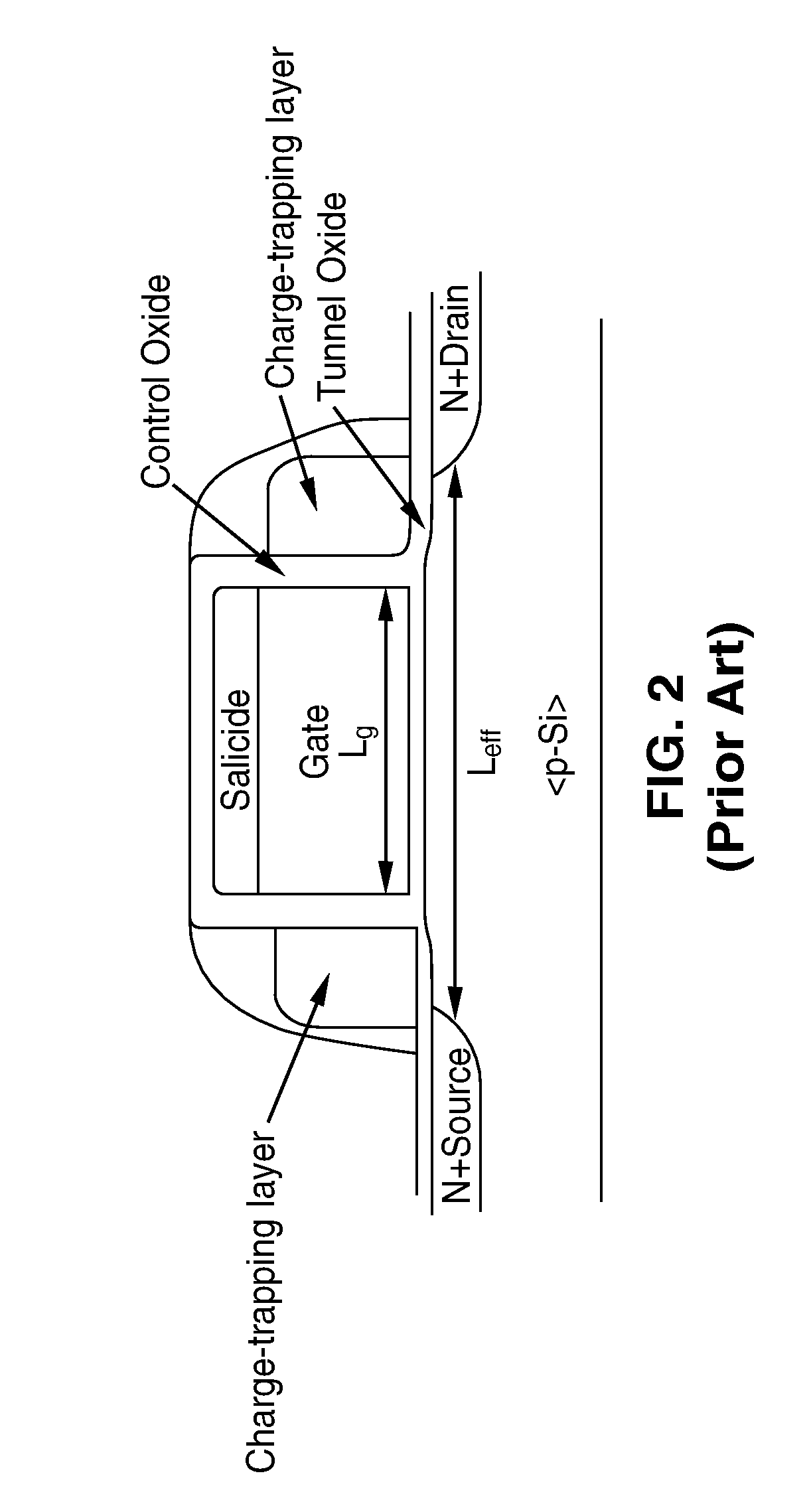
These technologies are difficult to scale to sub-50 nm Lg since the metric of choice (e.g., the cell's VT) is highly sensitive to short channel effects (SCE).
Specifically, the drain-induced barrier lowering (DIBL) effect makes VT of the cell sensitive to charge stored on the bit next to the drain electrode, and this sensitivity, which is normally referred to as the complementary bit disturb issue, affects the separation between programmed and erased states, and thus affects the scalability of the structure.
This requirement limits the potential scalability of this structure since its effective gate-length (Leff) must be significantly larger than its actual gate-length (Lg).

Method used


Image

  • Multi-bit-per-cell nvm structures and architecture
  • Multi-bit-per-cell nvm structures and architecture
  • Multi-bit-per-cell nvm structures and architecture

Examples


embodiment 50

[0102]FIG. 9 through FIG. 11, illustrate an embodiment 50 of the cell structure (FIG. 9-10) and an example array configuration (FIG. 11) for the NOR-type array architecture of FIG. 7. FIG. 9 depicts an XZ plane view of cell 50 while FIG. 10 is a YZ plane view of cell 50. FIG. 11 illustrates a layout (not to scale) in which an array of cells 50 are interconnected to word and bit lines.

[0103] The NVM array structure of FIG. 11 is fabricated on a silicon on insulator (“SOI”) material, which lies on top of a buried oxide (“BOX”) substrate 52, upon which bit lines BL0-BL7 are formed. The FinFET NVM cell 50 is formed on a p-type silicon on insulator (SOI) wafer, where silicon is (epitaxially) grown on top of a buried oxide (“BOX”) film 52 (hence, the term “SOI”). The fin 54 is made of p-type silicon, and bit-lines BL0, BL1 also comprise silicon, except that these are doped with n-type impurities, such as phosphorus, to make them “n-type”. The gate oxide film 60 preferably comprises silico...

embodiment 70

[0110]FIG. 16-19 shows a basic layout (not to scale) of an embodiment 70 of a cell structure (with planar cross-sections) of the unit cell and a NAND-type array architecture 84. As shown, this architecture uses SOI technology, and the unit cell in this architecture is the DG SONOS NVM FinFET cell structure according to an embodiment of the invention, although the architecture applies to structures shown in FIG. 4A-4B.

[0111] A SOI substrate, which lies on top of a BOX layer 72 is used to form each NVM FinFET cell 70. In this embodiment, fin 74 comprises p-type silicon, while bit-lines BL0, BL1 also comprise silicon which is doped with n-type impurities, such as phosphorus, to make them “n-type”. In this double-gated structure, the top of fin 74 is further isolated from the word-line with a thick silicon dioxide film 76, which provides a hard-mask in the manufacturing process of the cell. By way of example, the gate oxide film 82 comprises silicon dioxide (SiO2), and the charge-trappi...

embodiment 90

[0128] A SOI substrate, which lies on top of a BOX layer 92 is used to form this novel NVM FinFET cell 90. The materials and processes for embodiment 90 are described by way of example, and not limitation. Fin 94 comprises p-type silicon, with source electrode 96a and drain electrode 96b comprising silicon doped with n-type impurities, such as phosphorus, to make them “n-type”. The source 96a and drain 96b electrodes of the cell are connected to the memory array bit-lines (BL). This structure contains four ONO gate-dielectric stacks (98, 102, 104, and 106), each stack containing a tunneling silicon dioxide (SiO2) film 100a, which isolates a silicon nitride (Si3N4) charge-trapping region 100b. A silicon dioxide (SiO2) film 100a is used to isolate each charge-trapping film 100bfrom the (n+ PolySi) gate connected to the word-line (WL) of the array, as well as from the source-drain structure connected to the bit-line.

[0129] An exemplary process for fabricating the structure of FIG. 24-2...


PUM


Abstract

A transistor structure, such as a Double-gated FET (DG FET), that has been modified to include a charge-trapping region used to store either 2- or 4-bits of information. The charge-trapping region can, for example, be embedded in the gate dielectric stack underneath each gate electrode, or placed on the sidewalls of each gate electrode.

Description

CROSS-REFERENCE TO RELATED APPLICATIONS [0001] This application claims priority from U.S. patent application Ser. No. 60 / 749,735 filed on Dec. 12, 2006, incorporated herein by reference in its entirety.STATEMENT REGARDING FEDERALLY SPONSORED RESEARCH OR DEVELOPMENT [0002] Not Applicable INCORPORATION-BY-REFERENCE OF MATERIAL SUBMITTED ON A COMPACT DISC [0003] Not Applicable NOTICE OF MATERIAL SUBJECT TO COPYRIGHT PROTECTION [0004] A portion of the material in this patent document is subject to copyright protection under the copyright laws of the United States and of other countries. The owner of the copyright rights has no objection to the facsimile reproduction by anyone of the patent document or the patent disclosure, as it appears in the United States Patent and Trademark Office publicly available file or records, but otherwise reserves all copyright rights whatsoever. The copyright owner does not hereby waive any of its rights to have this patent document maintained in secrecy, ...

Claims


Application Information

Patent Timeline
Patent Type & Authority Applications(United States)
IPC IPC(8): H01L29/792G11C16/04
CPCG11C11/5671G11C16/0475G11C16/0483G11C16/0491H01L29/7923H01L27/11519H01L27/11521H01L29/785H01L29/7887H01L27/115H10B41/10H10B69/00H10B41/30H10B43/10
Inventor PADILLA, ALVAROKING, TSU-JAE
Owner RGT UNIV OF CALIFORNIA
Learn More