Printed circuit board for semiconductor package and method of manufacturing the same

a technology of printed circuit board and semiconductor package, which is applied in the direction of printed circuit manufacturing, resist details, printed circuit aspects, etc., can solve the problems of long time period for completing a final design, and inability to meet the requirements of final design, etc., and achieve the effect of fine pitch and inexpensive manufacturing of a pcb

Inactive Publication Date: 2007-07-26
SAMSUNG ELECTRO MECHANICS CO LTD
View PDF14 Cites 15 Cited by
  • Summary
  • Abstract
  • Description
  • Claims
  • Application Information

AI Technical Summary

Benefits of technology

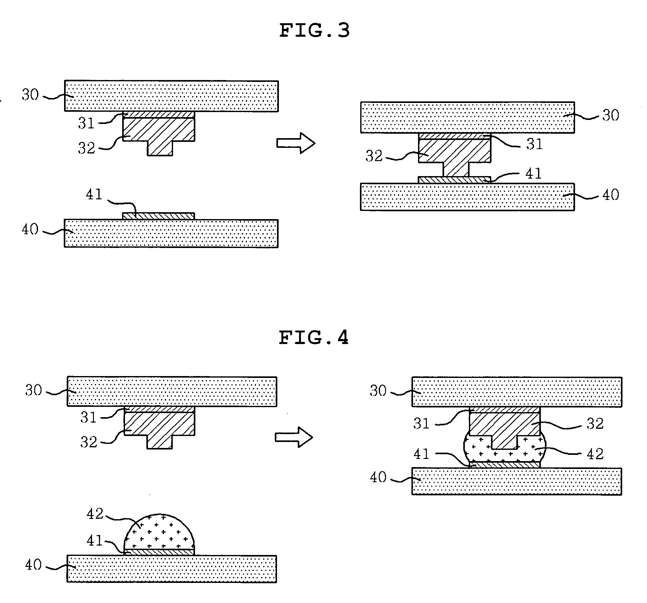
[0013]Leading to the present invention, intensive and thorough research into PCBs for packages, carried out by the present inventors aiming to avoid the problems encountered in the related art, resulted in the finding that a pre-solder may be formed on the bump of a PCB using a tin or tin alloy electroplating process, thereby inexpensively manufacturing a PCB for a package able to realize a fine pitch.
[0014]Therefore, one aspect of the present invention is to provide a PCB for a semiconductor package and a manufacturing method thereof, in which a fine pitch may be realized through an economical process.
[0015]Another aspect of the present invention is to provide a PCB for a semiconductor package and a manufacturing method thereof, in which it is easy to increase the height of a pre-solder to thus enhance bondability and underfilling capability.

Problems solved by technology

However, in the case where the RDL should be formed for conversion into the array type, circuit interference occurs due to the formation of narrow circuits, undesirably increasing the noise generation rate.
Thereby, there is a need for verification through simulation and performance tests, resulting in a long time period for completing a final design.
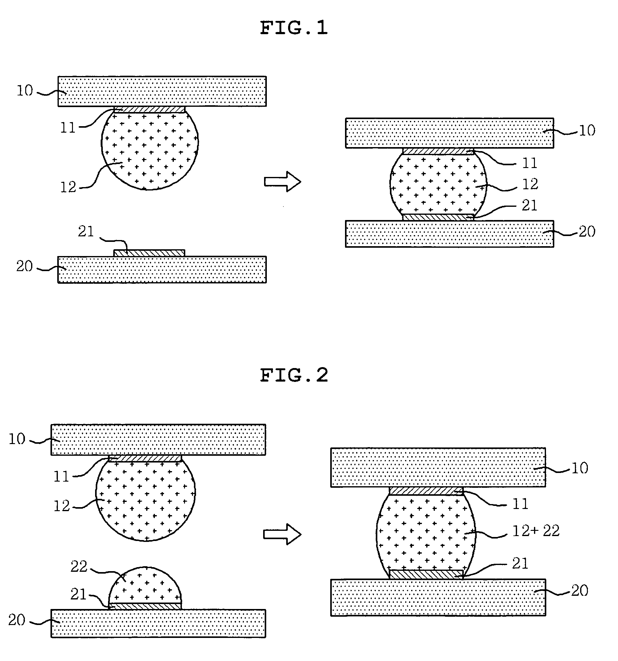
However, in the conventional pre-solder formation techniques, the screen printing method suffers because it is difficult to realize a pre-solder of 120 μm pitch or less.
In addition, although the super juffit method and the super solder method may be applied even to a fine pitch of 100 μm pitch or less, they incur high costs.

Method used


Image

  • Printed circuit board for semiconductor package and method of manufacturing the same
  • Printed circuit board for semiconductor package and method of manufacturing the same
  • Printed circuit board for semiconductor package and method of manufacturing the same

Examples


example 1

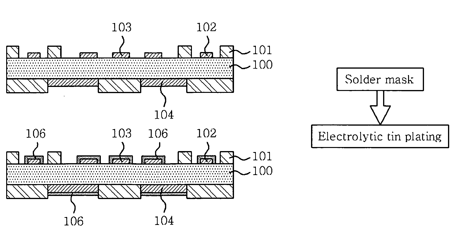
[0070]In the product as in FIG. 7, all of a soldering portion, a bump portion, and a wire bonding portion having a mark recognizable to a camera and a mold gate for molding after mounting were subjected to tin plating. In particular, the pitch of the bump portion was set within a range of 40˜200 μm, and the thickness of the plating layer was changed depending on the pitch. In the present example, in the case of 100 μm pitch, since a bump copper circuit interval was small, in the vicinity of about 30 μm, the tin plating was performed to a target thickness of 10 μm. To this end, using a PC-MT plating solution available from Incheon Chemical, Korea, the plating process was performed at 25° C. for 25 min at 1.0 ASD, resulting in a plating layer composed of at least 99% pure tin. Additionally, the plating process was conducted at 25° C. for 12 min at 3 ASD using a UTB-TS 140 plating solution, available from Ishihara Chemical, Japan, resulting in a plating layer composed of 97.5% Sn and 2...

example 2

[0071]In the product as in FIG. 8, among a soldering portion, a bump portion, and a wire bonding portion having a mark recognizable to a camera and a mold gate for molding after mounting, only the bump portion was subjected to tin plating. The copper pads, other than the bump portion, were subjected to nickel and gold plating. As such, the bump portion was masked with a dry film so as not to be plated. Subsequently, when the bump portion was subjected to tin plating, the portion of the substrate other than the bump portion was masked with a dry film such that the nickel and gold plated portion was not plated with tin. The thickness of the nickel plating layer was 2˜20 μm, which was as thick as a general nickel electroplating layer. In particular, the pitch of the bump portion was set within a range of 40˜200 μm, and the thickness of the plating layer was changed depending on the pitch. In the present example, in the case of 100 μm pitch, since a bump copper circuit interval was smal...

example 3

[0072]In the product as in FIG. 9, among a soldering portion, a bump portion, and a wire bonding portion having a mark recognizable to a camera and a mold gate for molding after mounting, only the bump portion was subjected to tin plating. All the copper pads were subjected to nickel and gold plating. Subsequently, when the bump portion was subjected to tin plating, part of the substrate other than the bump portion was masked with a dry film such that a nickel and gold plating layer and then a tin plating layer were formed only on the bump portion. In particular, the pitch of the bump portion was set within a range of 40˜200 μm, and the thickness of the plating layer was changed depending on the pitch. In the present example, in the case of 100 μm pitch, since a bump copper circuit interval was small, in the vicinity of about 30 μm, the nickel plating layer was formed to a thickness of 1.0 μm, which was less than the thickness of a general nickel electroplating layer. Further, the t...


PUM


Abstract

Disclosed are a printed circuit board for a semiconductor package and a method of manufacturing the same. Specifically, a printed circuit board for a semiconductor package includes predetermined circuit patterns, having a wire bonding portion and a bump portion for mounting a semiconductor and a soldering portion for connection to external parts, in which the bump portion has a pre-solder formed using a tin or tin alloy electroplating process. According to this invention, the pre-solder, which is formed by reflow using an electroplating process, permits easy increase of the height thereof to thus enhance bondability and underfilling capability, may be formed to a desired thickness by controlling a plating thickness, and furthermore, may be applied to a fine pitch through a masking process.

Description

CROSS REFERENCE TO RELATED APPLICATION(S)[0001]This application claims the benefit of Korean Patent Application No. 10-2006-0006854, entitled “Method for manufacturing printed circuit board for semi-conductor package and printed circuit board manufactured therefrom”, filed Jan. 23, 2006, which is hereby incorporated by reference in its entirety into this application.BACKGROUND OF THE INVENTION[0002]1. Field of the Invention[0003]The present invention relates, in general, to a printed circuit board (PCB) for a semiconductor package and a method of manufacturing the same. More particularly, the present invention relates to a PCB for a semiconductor package, in which a pre-solder can be formed on a bump portion using a tin or tin alloy electroplating process to thus enhance bondability and underfilling capability, and can be formed to a desired thickness by controlling a plating thickness, and in which it is possible to realize fine pitch, and to a method of manufacturing the same.[000...

Claims


Application Information

Patent Timeline
Patent Type & Authority Applications(United States)
IPC IPC(8): H01L23/48
CPCH05K2203/0723H01L23/49816H01L2924/01327H01L23/49866H01L2224/16H01L2924/01077H01L2924/01078H01L2924/01079H05K3/243H05K3/244H05K3/3463H05K3/3473H05K3/3489H05K2201/0391H05K2203/043H05K2203/0574H01L2224/81191H01L2224/81193H01L2924/00H01L2224/05573H01L2224/05568H01L2924/00014H01L2224/05599H05K1/09
Inventor LEE, YONG BINBAE, KYOUNG WONCHOI, JONG MINYOO, EUI YOUN
Owner SAMSUNG ELECTRO MECHANICS CO LTD
Why Eureka
Try Eureka