Method of manufacturing ink jet recording head

Inactive Publication Date: 2007-08-02
CANON KK
15 Cites 24 Cited by

AI-Extracted Technical Summary

Problems solved by technology

The manufacturing method described above is one excellent in utility, but an ink discharge rate is very small, and has a limitation in dimension designing because the finished dimension tolerances of the adhesive layers and the wall members of the flow pa...

Benefits of technology

[0015]The present invention was made in consideration of the aforesaid respects. It is an object of the present invention to provide a method of manufacturing an ink jet recording head tha...

Abstract

A method of manufacturing an ink jet recording head includes the steps of: forming an adhesive layers and the side walls of a flow path on a substrate; pasting a dry film, which is a part of a flow path forming member, on the side walls; and forming discharge ports in the layer.

Application Domain

Technology Topic

Image

  • Method of manufacturing ink jet recording head
  • Method of manufacturing ink jet recording head
  • Method of manufacturing ink jet recording head

Examples

  • Experimental program(3)

Example

First Embodiment
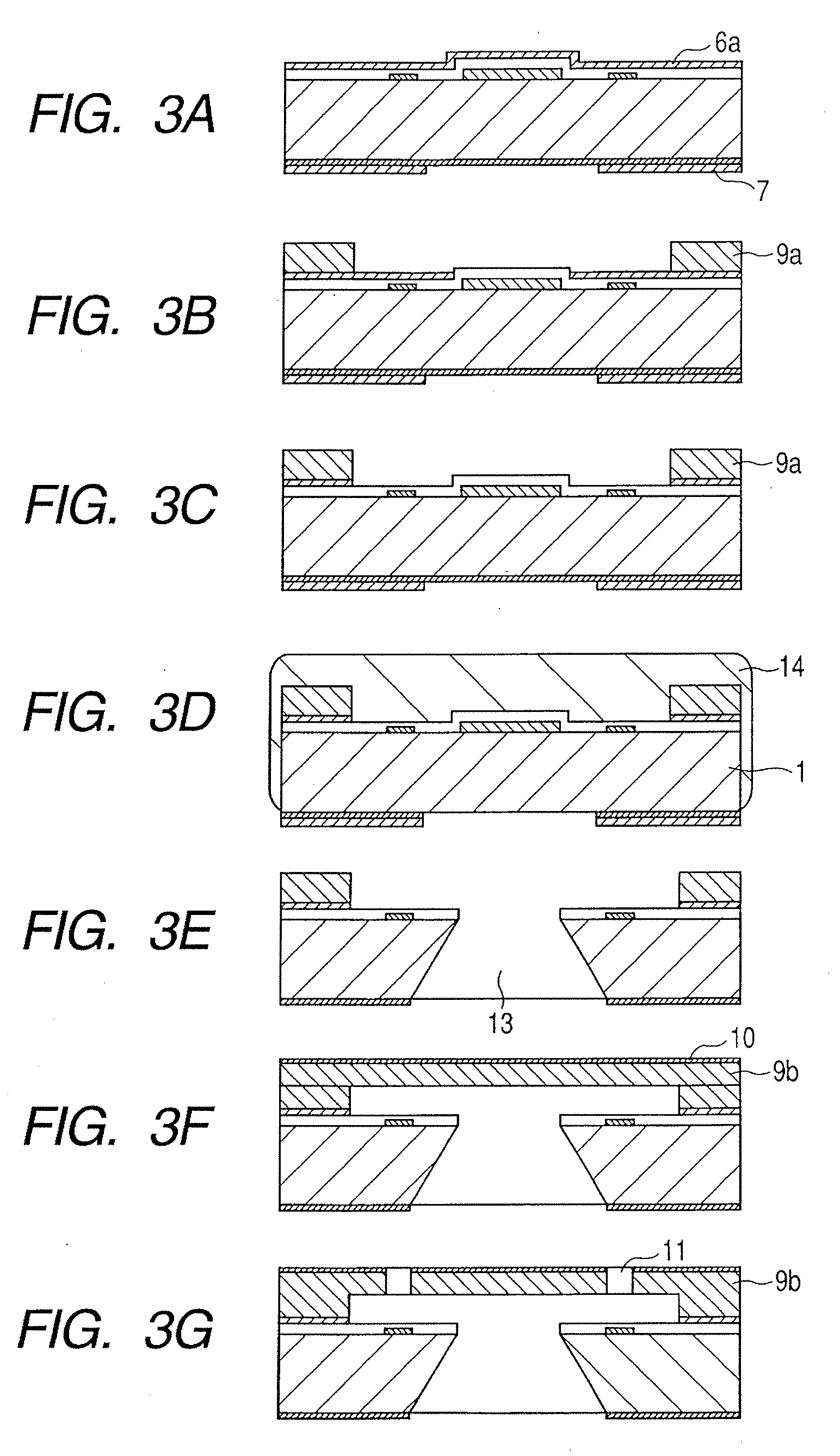
[0035]First, an adhesive material for forming the adhesive layers 6 on the substrate 1 equipped with the energy generating elements 2 is laminated (adhesive material lamination process).
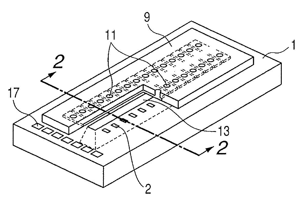
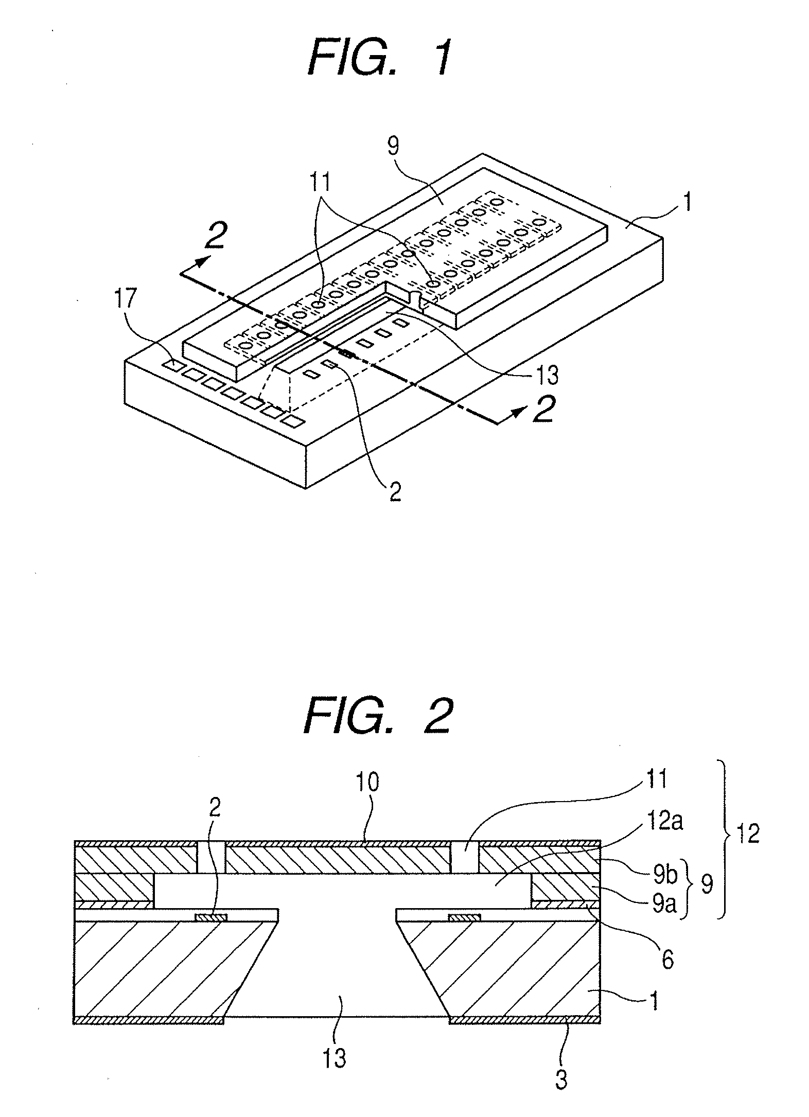
[0036]First, a plurality of the energy generating elements 2 such as heating resistors or the like is formed in, for example, parallel two rows at the predetermined pitch, as described above, on the front surface of the substrate 1, which is made of silicon or the like, and the whole back surface of which is covered by a SiO2 film 3. Electrodes and wiring for supplying electric power to drive the energy generating elements 2 arranged in parallel two rows are connected to the energy generating elements 2. Moreover, a sacrifice layer 5 is formed between the energy generating elements 2. The sacrifice layer 5 is formed in order to suppress the increases of the errors of the calibers of the apertures on the upper side of the substrate 1, which errors are caused by the changes of the thickness of the substrate 1, in the case where the through-hole to be the ink supply port 13 is formed by the anisotropic etching, and it is preferable to form the sacrifice layer 5 with a material having a quality of dissolving into a solution used for the anisotropic etching. As such a material having the dissolving quality, there can be cited polysilicon, and aluminum, aluminum silicon, aluminum copper and aluminum silicon copper, the etching speeds of which are fast, in the case where the solution used for the anisotropic etching is a strong alkali solution such as tetramethyl ammonium hydroxide (TMAH). The protective film 4 having the quality described above is formed on the silicon substrate 1, on which the energy generating elements 2 and the sacrifice layer 5 have been formed. In addition, their descriptions and the illustrating are omitted.
[0037]As shown in FIG. 3A, an adhesive material 6a to form the adhesive layers 6 is laminated on the protective film 4. At this process, the adhesive material 6a is made to be in the laminated state, and the patterning to form the adhesive layers 6 is not performed. The method of forming the adhesive material 6a is that of dissolving polyether amide resin into a solvent, and then heating the solution to form the adhesive material 6a. Alternatively, the adhesive material 6a can be formed by dissolving a resin containing the epoxy resin and a curing agent into a solvent and by performing its coating and curing to form a film. These adhesive layers 6 can be formed as the need arises, and their thicknesses are suitably to be within a range of from about 2 to about 3 μm.
[0038]Resin layers 7 to be the mask layers of the anisotropic etching are formed on the back surface of the substrate 1. The resin layers 7 are formed by coating a solution of a polyether amide resin with a spin coater or the like, by heating and curing the solution, and by patterning the cured layer. Solutions of resins other than the polyether amide resin can be also used.
[0039]Next, as shown in FIG. 3C, a flow path forming material 8 containing a photosensitive resin is laminated on the adhesive layer material 6a to form the side walls 9a of the flow path 12a by exposure and development (side wall forming process).
[0040]Because the material for forming the flow path forming member contains the photosensitive resin, it becomes possible to perform the patterning by the photolithography. Such a flow path forming material 8 is coated on the adhesive layer material 6a by, for example, the spin coat method.
[0041]After the coating, the flow path forming material 8 is exposed and cured by an ultraviolet ray, a deep UV ray or the like through the mask. After that, the flow path forming material 8 is developed to be formed as the flow path side walls 9a as shown in FIG. 3C. After that, using the flow path side walls 9a as the mask, the adhesive layer material 6a is etched by the dry etching or the like, and is removed, only the portions existing between the flow path side walls 9a and the substrate 1 remaining. Thus, the adhesive layers 6 are formed.
[0042]Next, a through-hole to be the ink supply port 13 is formed from the back surface side of the silicon substrate 1 (ink supply port forming process). In addition, the timing of performing the process is not essential to the present invention, and the process may be performed after a discharge port forming process shown in FIG. 3G.
[0043]As shown in FIG. 3D, the front surface and the side surface of the substrate 1 are covered by a protective material 14 by the spin coat method or the like. The protective material 14 is provided for protecting the ink chamber side wall members from the damages at the time of conveyance, and for producing an etching resistant property at the time of forming the ink supply port 13 from the back surface of the substrate 1.
[0044]The SiO2 film 3 on the back surface of the substrate 1 is etched using the polyether amide resin layers 7 as the mask, and the portion of the substrate 1 that is the starting surface of the etching to form the through-hole of the substrate 1 in order to form the ink supply port 13 is exposed.
[0045]As shown in FIG. 3E, the etching is performed from the etching starting surface formed on the back surface of the substrate 1, and the through-hole to become the ink supply port 13 is formed. Such etching may be performed by any of the methods of the dry etching, the etching using an excimer laser, the wet etching, and a combination of them, but the anisotropic etching by the wet etching is preferable because it can be easily performed. A strong alkali solution such as the solution of TMAH can be used for the anisotropic etching. The through-hole is formed in the substrate 1, and continuously the isotropic etching of the sacrifice layer 5 formed on the front surface of the substrate 1 is performed to form the ink supply port 13. After that, the resin layers 7 and the protective material 14 on the back surface of the substrate 1 are removed.
[0046]Next, a layer constituting a part of the flow path forming member is pasted on the side walls of the flow path 12a of the substrate 1 (layer pasting process).
[0047]As shown in FIG. 3F, the layer constituting the ceiling member 9b of the ink chamber is pasted on the side wall members 9a. Any layer constituting 9b may be used as the layer as long as it has rigidity at the degree capable of being not bent when it is placed on the side walls 9a. As the quality of material of the layer constituting 9b, for example, a material containing a photosensitive resin and a photo cationic polymerization initiator is preferable because it makes it possible to form the ink discharge ports 11 by the development by the photolithography without performing any etching. Moreover, the quality of material of the dry film preferably has the same composition as those of the flow path side walls 9a. For example, if the side walls 9a are cured materials of the epoxy resin, the layer constituting 9b is preferably the one containing an epoxy resin and a curing agent. In particular, if the epoxy resins used for the side walls 9a and the epoxy resin contained in the layer constituting the ceiling member 9b are the same ones, it is further preferable.
[0048]It is preferable to laminate the water repellency agent layer 10 on the front surface of the layer 9b.
[0049]Next, as shown in FIG. 3G, the ink discharge ports 11 are formed in the layer (discharge port forming process). The formation is performed by exposing the dry film and curing the exposed portions. By the curing, the joining between the side walls 9a and the ceiling member 9b becomes more firm. If the materials of the side walls 9a and the dry film are the same ones, more firm joining of both the materials can be obtained from the viewpoint of the affinity of both the materials.
[0050]Electric joining for driving the energy generating elements 2 of the ink jet recording head obtained by the processes mentioned above is performed. Then, the ink supply ports 11 is connected to the ink supply path 13 connected to the ink storage unit, and a unit of the ink jet recording head capable of being mounted on a recording apparatus can be completed.

Example

Second Embodiment
[0051]As a second embodiment of the present invention, a case of using a photosensitive material as the adhesive layers 6 is described with reference to FIGS. 5A to 5C.
[0052]As shown in FIG. 5A, the adhesive material 6a to form the adhesive layers 6 is laminated on the protective film 4. Hereupon, usable materials as an adhesive material 6b are, for example, polyether amide, a crosslinking agent to crosslink the polyether amide under the existence of a catalyst such as an acid, and a photosensitive material to generate the catalyst by being exposed. To put it more concretely, there can be cited a melamine compound as the crosslinking agent, and a material known as a photoacid generator as the photosensitive material. Moreover, as the other examples of the adhesive material 6b, there can be cited a negative type photosensitive resin material containing the epoxy resin and the photoacid generator, and the like.
[0053]The polyether amide resin layers 7 to be the mask layers of the anisotropic etching is formed on the back surface of the substrate 1. The polyether amide resin layers 7 are formed by coating the solution of the polyether amide resin with a spin coater or the like, and by heating and curing the coated solution. Then, cured solution is patterned to form the polyether amide resin layers 7.
[0054]Next, as shown in FIG. 5B, the flow path forming material 8 having photosensitivity is laminated on the adhesive material 6a. As the flow path forming material 8, a material containing the photoacid generator and the epoxy resin is suitably used, but the material is not limited to the one containing the photoacid generator and the epoxy resin. It is desirable that the photosensitive wavelengths of the adhesive material 6a and the flow path forming material 8 overlap each other for later processes.
[0055]Next, as shown in FIG. 5C, the adhesive material 6a and the flow path forming material 8 are patterned all at one time to form the side walls 9a (flow path side wall forming process). If the photosensitive wavelengths of both of the materials 6a and 8 overlap each other, the adhesive material 6a and the flow path forming material 8 can be exposed by one time light radiation in a lump. The selection of a developing solution in a development is arbitrary, but it is further effective to perform the development using the same developing solution all at one time. It is needless to say that the selection is not limited to that case, but the development may be performed separately using different developing solutions.
[0056]By the process mentioned above, the patterning of the side walls 9a and the adhesive layers 6 can be performed all at one time, and the flow path side walls 9a can be obtained by a simple process.
[0057]The processes on and after that can be performed similarly to those illustrated in FIG. 3D and after that of the first embodiment.

Example

[0058]A third embodiment of the present invention is described with reference to FIGS. 6A to 6D.
[0059]The present embodiment is an example of separating the process of forming the adhesive layers 6 and the process of forming the side walls 9a to increase the selectivity of the materials of both of them.
[0060]As shown in FIG. 6A, the adhesive material 6a to form the adhesive layers 6 is laminated on the protective film 4. As the adhesive material 6a, it is possible to use the adhesive materials described in the first and the second embodiments.
[0061]Next, as shown in FIG. 6B, the adhesive material 6a is patterned to form the adhesive layers 6. If the adhesive material 6a has photosensitivity, the patterning is performed by using the technique of photolithography. If the adhesive material 6a does not have the photosensitive, the patterning is performed by etching or the like.
[0062]Next, as shown inFIG. 6C, the flow path forming material 8 is laminated on the adhesive layers 6. As the flow path forming material 8, the materials shown in the first and the second embodiments can be suitably used.
[0063]Next, as shown in FIG. 6D, the flow path forming material 8 is patterned to form the flow path side walls 9a.
[0064]The processes on and after the one shown in FIG. 6D can be performed similarly to those illustrated in FIG. 3D and the drawings following to FIG. 3D of the first embodiment.
[0065]If the present embodiment is adopted, both of the photosensitive adhesive materials and non-photosensitive adhesive materials can be selected as the adhesive material 6a.
[0066]While the present invention has been described with reference to exemplary embodiments, it is to be understood that the invention is not limited to the disclosed exemplary embodiments. The scope of the following claims is to be accorded the broadest interpretation so as to encompass all such modifications and equivalent structures and functions.
[0067]This application claims the benefit of Japanese Patent Application No. 2006-025777, filed Feb. 2, 2006, which is hereby incorporated by reference herein in its entirety.

PUM

PropertyMeasurementUnit
Composition
Adhesivity
Energy
tensileMPa
Particle sizePa
strength10

Description & Claims & Application Information

We can also present the details of the Description, Claims and Application information to help users get a comprehensive understanding of the technical details of the patent, such as background art, summary of invention, brief description of drawings, description of embodiments, and other original content. On the other hand, users can also determine the specific scope of protection of the technology through the list of claims; as well as understand the changes in the life cycle of the technology with the presentation of the patent timeline. Login to view more.

Similar technology patents

Classification and recommendation of technical efficacy words

  • High accuracy
  • Low price
Why Eureka
Try Eureka