Integrated Circuit Device

a circuit device and integrated circuit technology, applied in the field of improved devices, can solve the problems of pinholes, microcracks, and other defects, and achieve the effect of improving device reliability and small geometries

Inactive Publication Date: 2007-08-09
LI CHOU H
View PDF35 Cites 32 Cited by
  • Summary
  • Abstract
  • Description
  • Claims
  • Application Information

AI Technical Summary

Benefits of technology

[0009] Therefore, to overcome the foregoing and other difficulties, the general object of this invention is to provide an improved, surface-passivated solid state device having very small geometries, with improved device reliability, mechanically, chemically, and electrically;

Problems solved by technology

These devices therefore often fail by surface or stress-related mechanical, and subsequently electronic failure mechanisms.
Unfortunately, these surface layers are far from being perfect or even inert, but are often full of pinholes, microcracks, and other defects.

Method used


Image

  • Integrated Circuit Device
  • Integrated Circuit Device

Examples


Embodiment Construction

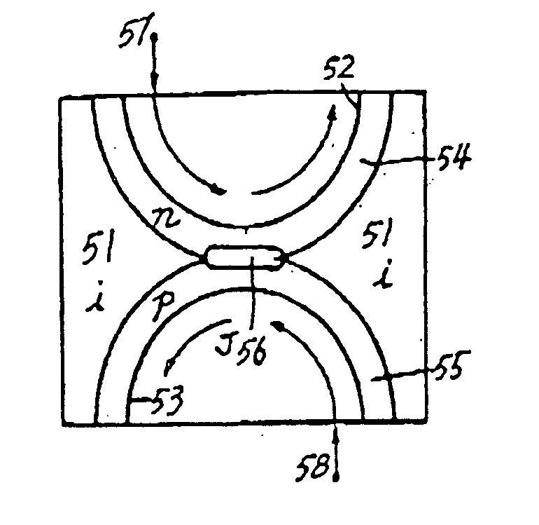
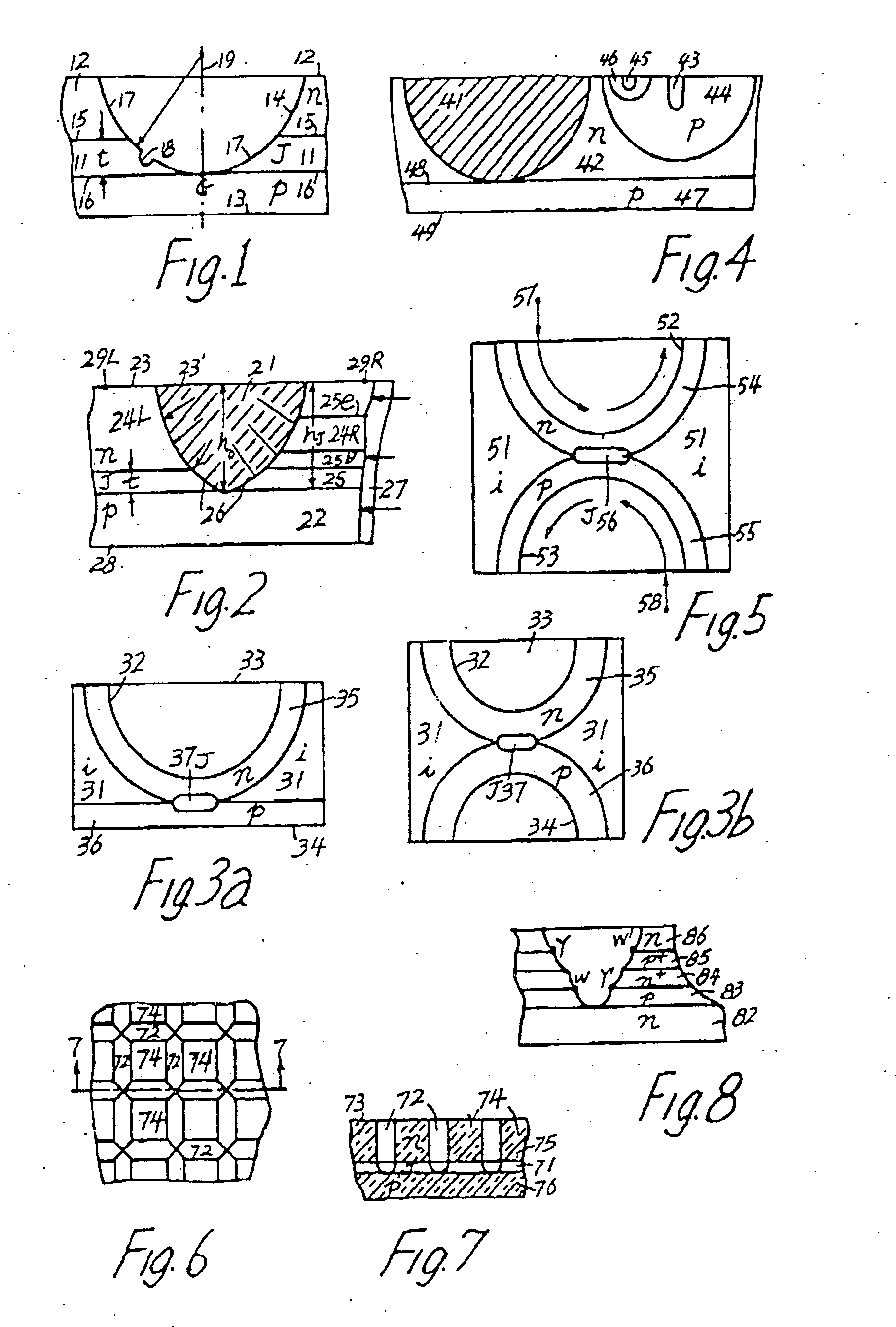
[0027] The PN junction devices of FIGS. 1-2 are sufficiently disclosed in the previously referenced patents and patent applications.

[0028] In the devices of FIGS. 1 and 2, the electrical signal current through the interfacial electronic barrier, such as a PN junction, is controlled by mobile carriers in the form of electrons and / or holes. The interfacial electronic barrier generally changes its electrically conductivity depending on the applied bias thereacross. For example, a PN junction is substantially electrically nonconductive under an applied reverse bias, but conductive under applied forward bias. That is, the PN junction is substantially either nonconductive or conductive under an applied bias of at least one selected polarity. This PN junction is a critical component in many, but not all, of the solid-state devices of the invention.

[0029] Other than PN junctions, metal-semiconductor or Schottky barriers, heterojunctions (e.g., between Si, SiC, or GaAs, and diamond), metal...


PUM


Abstract

A commercially mass-produced, integrated circuit including: a solid substrate of one conductivity type; at least one solid material pocket of a different conductivity type having a side surface and positioned on a selected top surface of the substrate to thereby form a signal-translating, electronic rectifying barrier between the at least one solid material pocket and the selected top surface of the substrate; and a solid state material region adjoining the substrate, the electronic rectifying barrier, and the side surface of the at least one solid material pocket; wherein next to the electronic rectifying barrier the solid state material region has a lateral dimensional accuracy of better than a few hundred atomic layers.

Description

CROSS-REFERENCE TO RELATED APPLICATIONS [0001] This application is a continuation-in-part of U.S. patent application Ser. No. 08 / 483,938 filed Jun. 7, 1995, entitled INTEGRATED CIRCUIT DEVICE, the entirety of which is hereby incorporated by reference.BACKGROUND OF THE INVENTION [0002] This invention is in the field of improved integrated circuit devices and specifically in the field of miniaturized dielectrically isolated integrated circuit devices. [0003] Solid-state devices in general and semiconductor devices in particular must have exacting surface properties for successful operations. These devices therefore often fail by surface or stress-related mechanical, and subsequently electronic failure mechanisms. The surface of a PN, P+N, P−N, PN+, PN−, PI, NI, metal-oxide, metal-semiconductor, oxide-semiconductor, interfacial rectifying barrier, and heterojunction between different semiconductor materials such as Si on SiC or diamond, or other optoelectromagnetically active signal-tr...

Claims


Application Information

Patent Timeline
Patent Type & Authority Applications(United States)
IPC IPC(8): H01L29/76H01L35/28H01L29/06H01L29/861H01L29/872
CPCH01L21/761H01L21/7621H01L29/0649H01L29/0657H01L29/0661H01L29/267H01S5/2072H01L29/872H01S5/02461H01S5/0424H01S5/183H01S5/2045H01L29/861
Inventor LI, CHOU H.
Owner LI CHOU H
Why Eureka
Try Eureka