MEMS device and manufacturing process thereof

a technology of microelectromechanical systems and manufacturing processes, applied in the field of microelectromechanical systems (mems) devices and manufacturing processes thereof, can solve the problems of reduced yield, cost increase, and special cavity forming and sealing steps of conventional mems devices

Inactive Publication Date: 2007-08-16
HITACHI LTD
View PDF12 Cites 160 Cited by
  • Summary
  • Abstract
  • Description
  • Claims
  • Application Information

AI Technical Summary

Benefits of technology

[0026]It is also possible to form a first slit in the L shape, T shape or cross shape in the lid (or diaphragm) and a second slit which is disposed in substantially parallel to at least one side of the L-shaped, T-shaped or cross-shaped slit, relax the stress of the thin film by elastic deformation of the beam sandwiched by these two slits, and seal the slits by the sealing film.
[0049]Moreover, the present invention makes it possible to provide a manufacturing process of an MEMS device capable of forming a thin film of a large area for the MEMS structure or a cavity of a large area for disposing the MEMS structure therein by employing a standard manufacturing step of CMOS LSI or a standard wiring step constituting the above-described step.

Problems solved by technology

A first problem to be overcome is that the conventional MEMS device needs special cavity forming and sealing steps.
This complicates the process and may cause problems such as fluctuations or variations in properties, reduction in yield, and cost increase.
As another sealing method by lamination, a method of having supports and bringing two wafers into contact at the supports is proposed, but this method is accompanied with the same problems.
A method of sealing using an LSI process, on the other hand, has difficulty in sealing a cavity of a large area owing to a residual stress of a sealing film serving as a lid.
More specifically, a sealing film of a large area may be broken or become uneven by the residual stress.
Poly Si subjected to stress relaxation at high temperatures is known as a film having a small residual stress, but it needs high heat processing so that it is not suited for MEMS or LSI integrated MEMS including metal interconnects.
When the sealing film is made thicker in order to heighten the mechanical strength of the lid, an increase in the influence of the stress cannot be ignored.
Existence of a difference in stress between thin films constituting the film stack may lead to appearance of unevenness in the lid (diaphragm).
Materials for the sealing film are therefore limited.

Method used


Image

  • MEMS device and manufacturing process thereof
  • MEMS device and manufacturing process thereof
  • MEMS device and manufacturing process thereof

Examples


first embodiment

[0069]A biaxial acceleration (vibration) sensor according to a first embodiment of the present invention will be described.

[0070]FIGS. 4A, 4B and 4C and FIGS. 5A, 5B and 5C are each a schematic cross-sectional view for explaining the manufacturing process of the sensor according to this embodiment, while FIGS. 6A and 6B are each a schematic view of a plane pattern in each layer of the main process step.

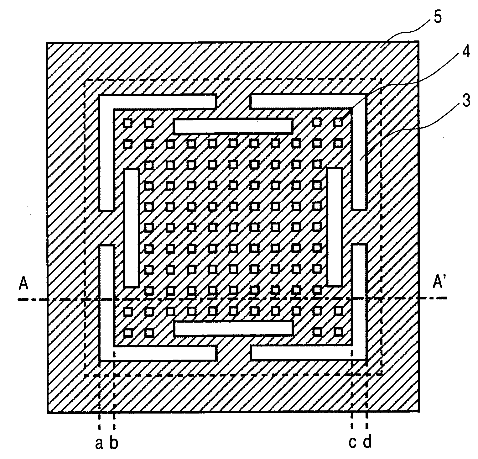
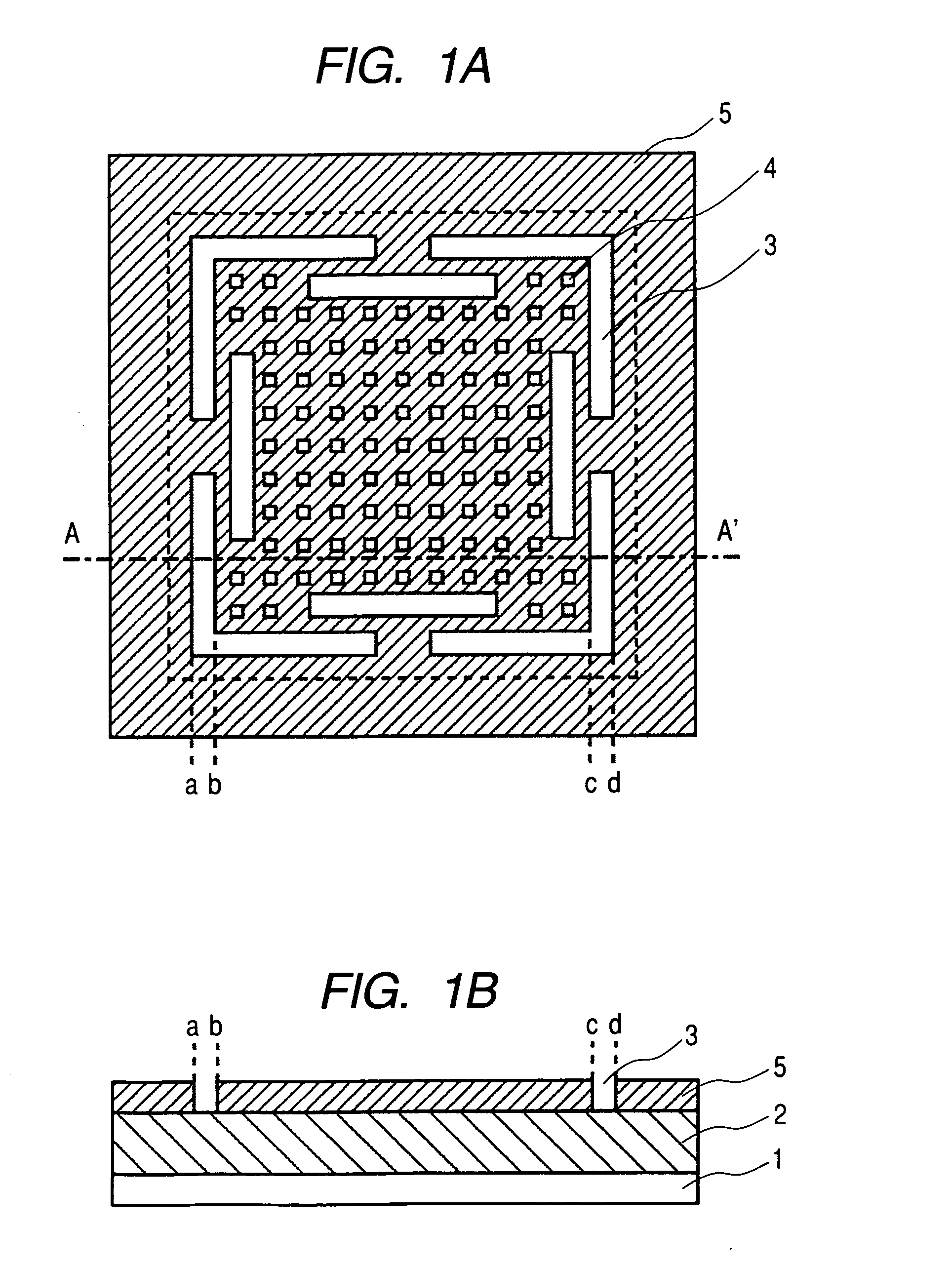
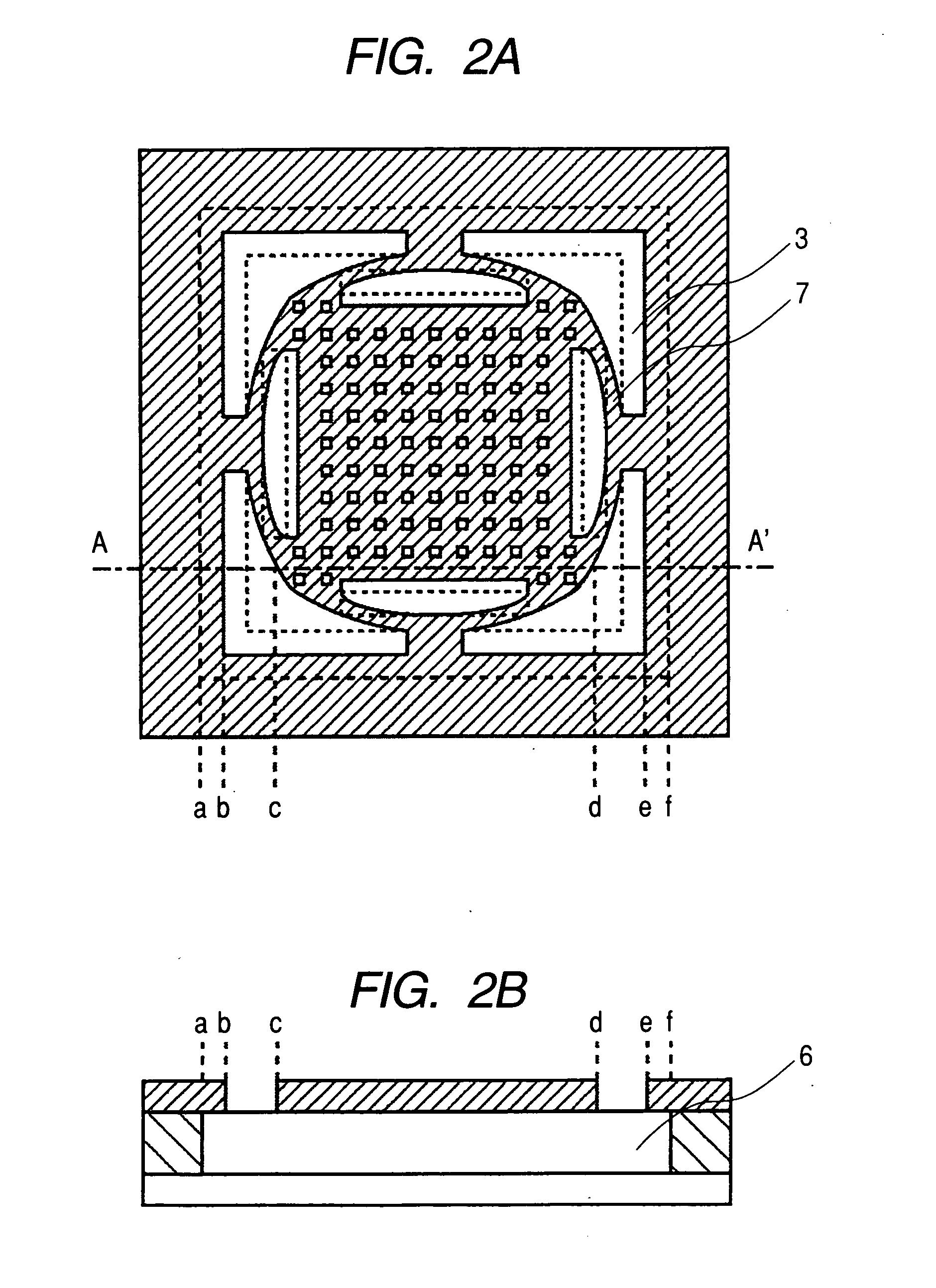
[0071]In accordance with the conventional process of a CMOS integrated circuit, a signal-processing integrated circuit transistor 102 for sensor, contact 103 and multilevel interconnects 104 are formed over a Si substrate 101. An interlayer film 106 made of a Si oxide film is formed over a fourth-level interconnect layer 105 by plasma CVD. After planarization by CMP (chemical mechanical polishing), a first sensor via 107 is formed (FIG. 4A). The first sensor via 107 connects between a predetermined interconnect of the fourth-level interconnect layer 105 and a first layer which will be...

second embodiment

[0086]An angular rate sensor (vibration gyroscope) according to a second embodiment of the present invention will next be described. In this Embodiment, a vibration body is formed by the SOI (Silicon On Insulator) process and then sealed by the LSI wiring process.

[0087]FIGS. 9, 10 and 18 are schematic views illustrating the planar configuration of a structure pattern in each layer constituting the vibration gyroscope, while FIG. 11 is a schematic view illustrating the manufacturing process of the vibration gyroscope according to this embodiment.

[0088]FIG. 9 is a plan view of the SOI layer constituting the vibration body. A layer corresponding to the first sensor layer of Embodiment 1 is also called “first sensor layer”. The first sensor layer pattern is a so-called vibration gyroscope sensor and it has a tuning-fork structure in which two vibration bodies subjected to vibration separation in an actuation (x) direction and a detection (y) direction have been coupled mechanically.

[008...

third embodiment

[0099]An application example of the present invention to an ultrasonic transducer will next be described as an application example to the formation of a diaphragm of a large area.

[0100]FIG. 12 is a schematic view illustrating the planar configuration of a pattern of a layer constituting a diaphragm of the ultrasonic transducer according to this embodiment, while FIGS. 13 and 14 are each a schematic view explaining the manufacturing process of the ultrasonic transducer according to this embodiment.

[0101]FIG. 12 is a plan view of a layer to be a lid of the cavity of the ultrasonic transducer (at the time of etching of a sacrificial layer). This layer corresponding to the second sensor layer of the second embodiment will hereinafter be also called second sensor layer. Different from the second sensor layer of the second embodiment, no minute etching holes are made in this embodiment. With regard to the cross-shaped slits, similar to those of the second embodiment, they have, at the nar...


PUM


Abstract

MEMS devices require special cavity formation and sealing steps such as wafer bonding which reduce the yield and increase the cost. In addition, it is difficult to form a cavity of a large area by the LSI process owing to a residual stress of a sealing film which will be a lid. This leads to a difficulty of realizing an integrated MEMS having a MEMS and a high-performance LSI mounted on one substrate. The lid (or diaphragm) covering therewith a cavity is equipped with slits or beams. During the formation of the cavity, the slits are deformed to absorb and relax the internal stress of the thin sealing film. Then, the cavity is sealed by filling the open portions of the film overlying the cavity between the inside and outside of the cavity. The cavity is formed by removing a portion of the interlayer film of LSI multilevel interconnects and the lid is made of a LSI-process thin film.

Description

CLAIM PRIORITY[0001]The present application claims priority from Japanese application JP 2006-035197 filed on Feb. 13, 2006, the content of which is hereby incorporated by reference into this application.FIELD OF THE INVENTION[0002]The present invention relates to a microelectromechanical systems (MEMS) device and manufacturing process thereof. In particular, the invention pertains to a technology effective when applied to a device having a semiconductor integrated circuit and MEMS integrated therein, a processing technology, and a sensor or switch utilizing the MEMS device.BACKGROUND OF THE INVENTION[0003]Microfabrication technology which has realized high-performance and high-integration semiconductor integrated circuits is now being utilized for the development of microelectromechanical systems (MEMS) technology for forming mechanical sensors, such as pressure sensors and accelerometers, and minute mechanical parts, such as microswitches and oscillators, and micromechanical syste...

Claims


Application Information

Patent Timeline
Patent Type & Authority Applications(United States)
IPC IPC(8): H01L21/00
CPCB81B7/0051B81C2203/0136B81C1/0023B81B3/0072
Inventor FUKUDA, HIROSHIWON, JEONG HEE
Owner HITACHI LTD
Why Eureka
Try Eureka