
Integrated circuit architecture for reducing interconnect parasitics

Inactive Publication Date: 2007-08-23
AGERE SYST INC
View PDF2 Cites 205 Cited by
  • Summary
  • Abstract
  • Description
  • Claims
  • Application Information

AI Technical Summary

Benefits of technology

[0006] The present invention meets the above-noted need by providing an improved integrated circuit architecture for reducing the effects of interconnect parasitics in an integrated circuit device and thereby improving circuit performance and reliability, particularly in deep submicron SoC designs. To accomplish this, in accordance with an illustrative embodiment of the invention, components or other circuits are distributed into at least two semiconductor chips, each semiconductor chip being used to handle different functional tasks. For example, a first chip, which may be referred to as a core chip, includes core components or other core circuits which will work cooperatively together as a system for handling core-related functional tasks. Similarly, a second chip, which may be referred to as an input / output (IO) chip, includes IO components or other IO circuits which will work cooperatively together for handling IO-related functional tasks. In this manner, the separate functional tasks can be independently optimized for improving overall integrated circuit performance.

Problems solved by technology

Signal integrity problems, such as, for example, crosstalk noise, current x resistance (IR)-drop and coupling-induced delay variation are becoming increasingly more significant due at least in part to the larger parasitics associated with an increasing number of interconnects and an increased circuit density in a given integrated circuit device.
At the same time, the complexity of implementing large systems on a chip is becoming increasingly burdensome on designers.
However, most circuit level solutions typically consume significant routing resources and usually result in a substantial increase in the number of iterations in the physical design loop, thereby undesirably increasing the design cycle of the integrated circuit and delaying time to market.
Both chip level and package level solutions, however, generally involve planar integration of functional blocks within the same chip, and therefore do not address signal integrity problems associated with global on-chip interconnects in advancing design technologies.

Method used


Image

  • Integrated circuit architecture for reducing interconnect parasitics
  • Integrated circuit architecture for reducing interconnect parasitics
  • Integrated circuit architecture for reducing interconnect parasitics

Examples


Embodiment Construction

[0013] The present invention will be described herein in the context of an illustrative SoC integrated circuit architecture. It should be understood, however, that the present invention is not limited to this or any other particular integrated circuit architecture and / or application. Rather, the invention is more generally applicable to techniques for providing an improved integrated circuit architecture for reducing the effects of interconnect parasitics in an integrated circuit device and thereby improve circuit performance and reliability, particularly in deep submicron SoC designs.

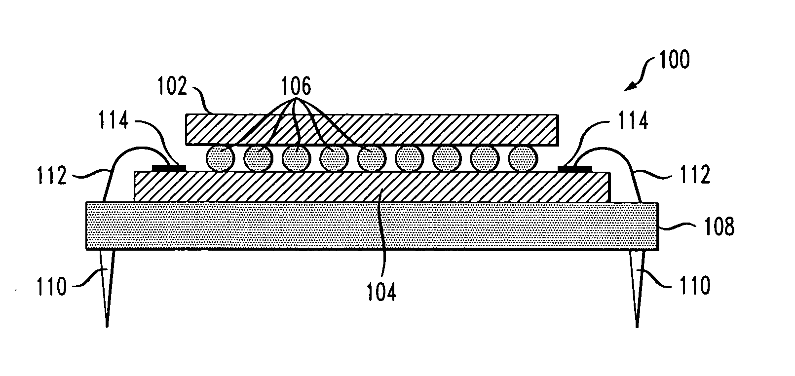
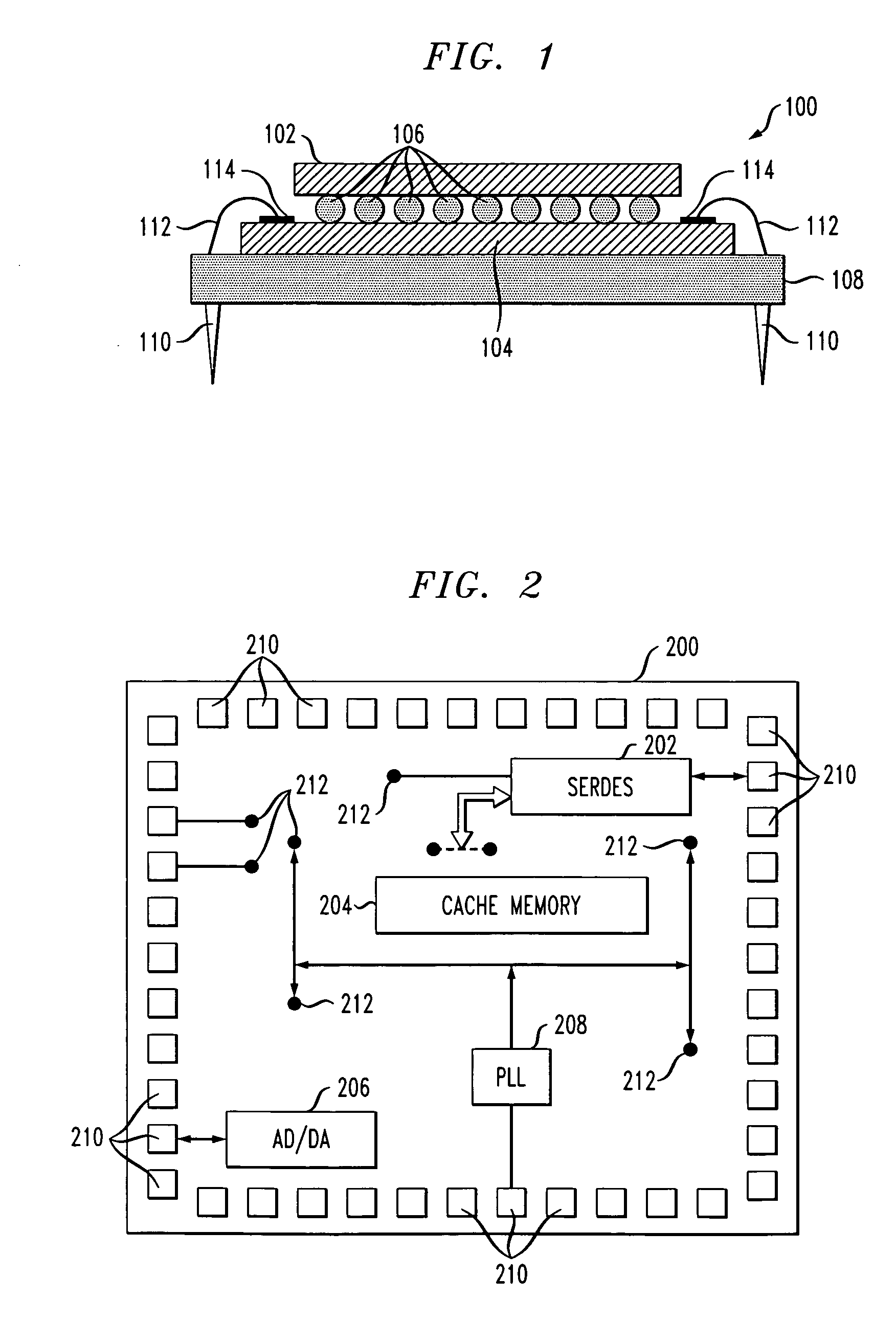
[0014]FIG. 1 is a cross-sectional view depicting an exemplary integrated circuit device 100, formed in accordance with one embodiment of the present invention. The integrated circuit device 100 comprises a first semiconductor chip 102 and at least a second semiconductor chip 104. Each of the semiconductor chips are preferably formed of silicon, and may therefore be referred to herein as silicon chips,...


PUM


Abstract

An integrated circuit includes a first semiconductor chip including one or more circuits thereon performing substantially core logic functions, the first semiconductor chip including multiple signal pads for providing electrical connection to the one or more circuits. The integrated circuit further includes at least a second semiconductor chip including one or more circuits thereon performing substantially input / output interface functions, the second semiconductor chip including multiple signal pads for providing electrical connection to the one or more circuits on the first semiconductor chip. The signal pads on the second semiconductor chip are substantially aligned with and electrically connected to corresponding signal pads on the first semiconductor chip. The first and second semiconductor chips are mutually functionally dependent on one another, such that at least a portion of at least one of the one or more circuits on the first semiconductor chip utilizes at least a portion of at least one of the one or more circuits on the second semiconductor chip, and vice versa. The first and second semiconductor chips are formed using first and second semiconductor fabrication processes, respectively.

Description

FIELD OF THE INVENTION [0001] The present invention relates generally to semiconductor devices, and more particularly relates to architectures for reducing the effects of interconnect parasitics in an integrated circuit device. BACKGROUND OF THE INVENTION [0002] As a consequence of the recent trend to push the lateral integration of systems on a chip (SoC), modern advanced application-specific integrated circuit (ASIC) design has focused largely on interconnects. This is due primarily to the fact that interconnects have become a dominant factor in determining circuit performance and reliability in deep submicron designs. Signal integrity problems, such as, for example, crosstalk noise, current x resistance (IR)-drop and coupling-induced delay variation are becoming increasingly more significant due at least in part to the larger parasitics associated with an increasing number of interconnects and an increased circuit density in a given integrated circuit device. At the same time, th...

Claims


Application Information

Patent Timeline
IPC IPC(8): H01L23/52H01L23/48H01L29/40
CPCH01L23/49575H01L24/10H01L24/13H01L2924/10253H01L2224/48247H01L2224/48227H01L2224/48091H01L25/18H01L2224/13099H01L2924/01077H01L2924/01322H01L2924/14H01L2924/1433H01L2924/01033H01L2924/014H01L2224/16145H01L2924/00014H01L2924/00H01L2224/13
Inventor CHAKRABORTY, KANADXU, BINGXIONGZHOU, XINGLING
Owner AGERE SYST INC
Features
  • Generate Ideas
  • Intellectual Property
  • Life Sciences
  • Materials
  • Tech Scout
  • Unparalleled Data Quality
  • Higher Quality Content
  • 60% Fewer Hallucinations
Learn More