Semiconductor device

a technology of semiconductor devices and semiconductors, applied in semiconductor devices, semiconductor/solid-state device details, instruments, etc., can solve problems such as chip size reduction, and achieve the effects of enhancing size reduction, mass productivity, reliability and signal transmission performan

Active Publication Date: 2007-08-23
RENESAS ELECTRONICS CORP
View PDF0 Cites 13 Cited by
  • Summary
  • Abstract
  • Description
  • Claims
  • Application Information

AI Technical Summary

Benefits of technology

[0010]It is possible to enhance a size reduction and mass productivity

Problems solved by technology

Further, since the controller section is originally small in circuit scale,

Method used


Image

  • Semiconductor device
  • Semiconductor device
  • Semiconductor device

Examples


Embodiment Construction

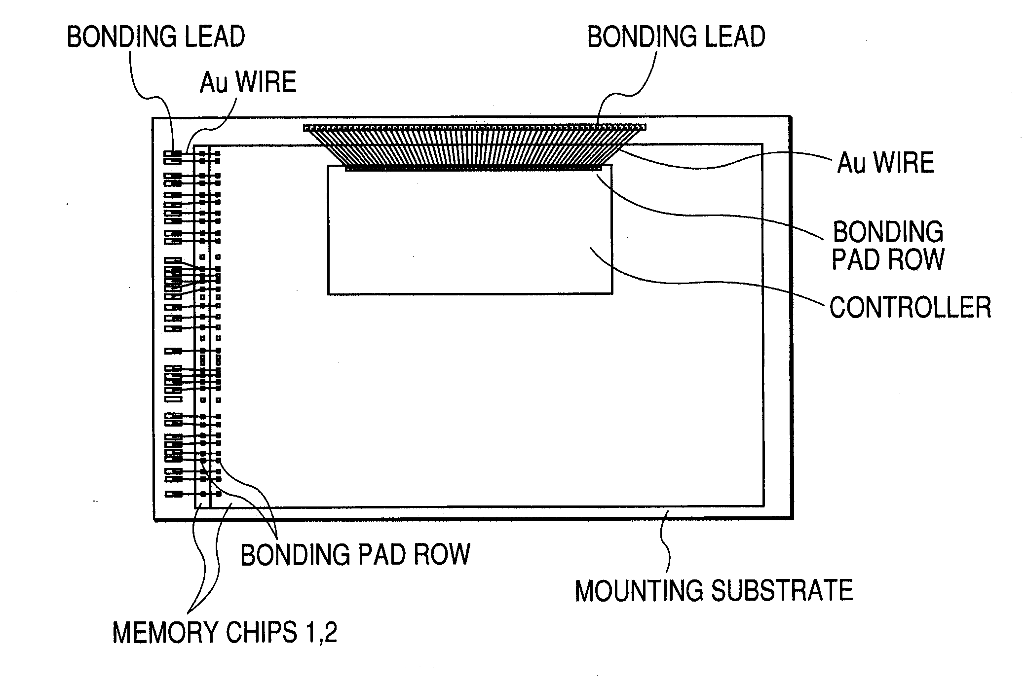
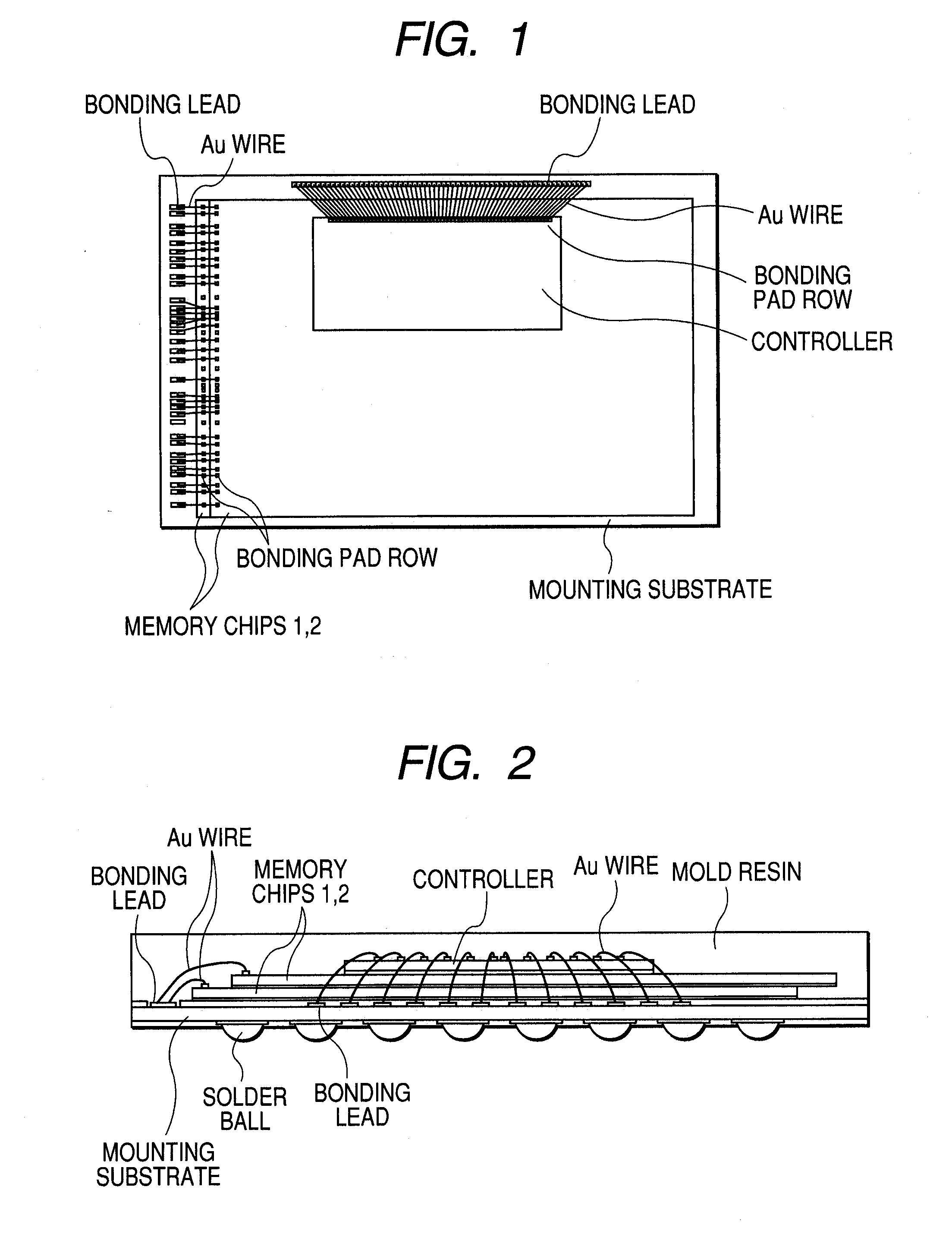
[0026]FIG. 1 shows a plan view of one embodiment of an MCP (SiP) as a nonvolatile memory device according to the present invention. FIG. 2 shows a schematic section thereof. In FIGS. 1 and 2, the MCP according to the present embodiment includes, although not restricted in particular, flash type two nonvolatile memories (hereinafter called simply memory chips 1 and 2) having a large storage capacity like an AG-AND type, and a controller including a CPU (Central Processing Unit) and a buffer memory, which are configured on a mounting substrate in the form of a layered structure.

[0027]Although not restricted in particular in the two memory chips 1 and 2, bonding pad rows are disposed along one short side of four sides. According to the relationship with the mounting substrate, the sides of the memory chips in which such bonding pad rows are disposed, are disposed in such a manner that the bonding pad rows correspond to bonding leads (electrode row) disposed along the left side of the m...


PUM


Abstract

This invention is to provide a nonvolatile memory device that enhances a size reduction and mass productivity while ensuring reliability and signal transmission performance. A nonvolatile memory chip having a first side formed with no pads and a second side formed with pads is mounted on a mounting substrate. A control chip for controlling the nonvolatile memory chip is mounted on the nonvolatile memory chip. The control chip has a first pad row corresponding to the pads of the nonvolatile memory chip. The first pad row is mounted adjacent to the first side of the nonvolatile memory chip. The first pad row of the control chip and a first electrode row formed on the mounting substrate are connected via a first wire group. The pads of the nonvolatile memory chip and a second electrode row formed on the mounting substrate are connected via a second wire group. The first electrode row and the second electrode row are connected through wirings formed in the mounting substrate.

Description

CROSS-REFERENCE TO RELATED APPLICATION[0001]The present application claims priority from Japanese patent application No. 2006-45463 filed on Feb. 22, 2006, the content of which is hereby incorporated by reference into this application.BACKGROUND OF THE INVENTION[0002]The present invention relates to a nonvolatile memory device, and to a technique effective if applied to a nonvolatile memory device of a multichip package (MCP) structure comprising, for example, a flash memory chip and a controller chip.[0003]As examples each illustrative of a semiconductor device in which a plurality of semiconductor chips are laminated and sealed with a resin, there have been known those disclosed in Japanese Unexamined Patent Publication No. 2001-102515 (patent document 1) and Japanese Unexamined Patent Publication No. 2001-217383 (patent document 2). Japanese Unexamined Patent Publication No. 2001-102515 is directed to the invention wherein two semiconductor chips identical in size and bonding pad...

Claims


Application Information

Patent Timeline
IPC IPC(8): H01L23/52
CPCG11C5/06H01L24/45H01L2924/10253H01L2224/48227H01L2924/01037H01L2224/32225H01L2924/3011H01L2924/30107H01L2924/15311H01L2924/01079H01L2924/01014H01L2924/01004H01L2225/06586H01L2225/06562H01L2225/06555H01L2225/0651H01L2225/06506H01L2224/73265H01L2224/49171H01L2224/48147H01L2224/48145H01L2224/48091H01L2224/45144H01L2224/32145H01L25/18H01L2924/00014H01L2924/00012H01L2924/00H01L24/73H01L2924/181H01L25/065
Inventor HANAWA, KAZUKOKIKUCHI, TAKASHIKANEMOTO, KOICHISUGIYAMA, MICHIAKIIMURA, CHIKAKO
Owner RENESAS ELECTRONICS CORP
Why Eureka
Try Eureka