

Anisotropic optical device and method for making same
- Summary
- Abstract
- Description
- Claims
- Application Information
AI Technical Summary
Benefits of technology
Problems solved by technology
Method used
Image

Examples
specific examples
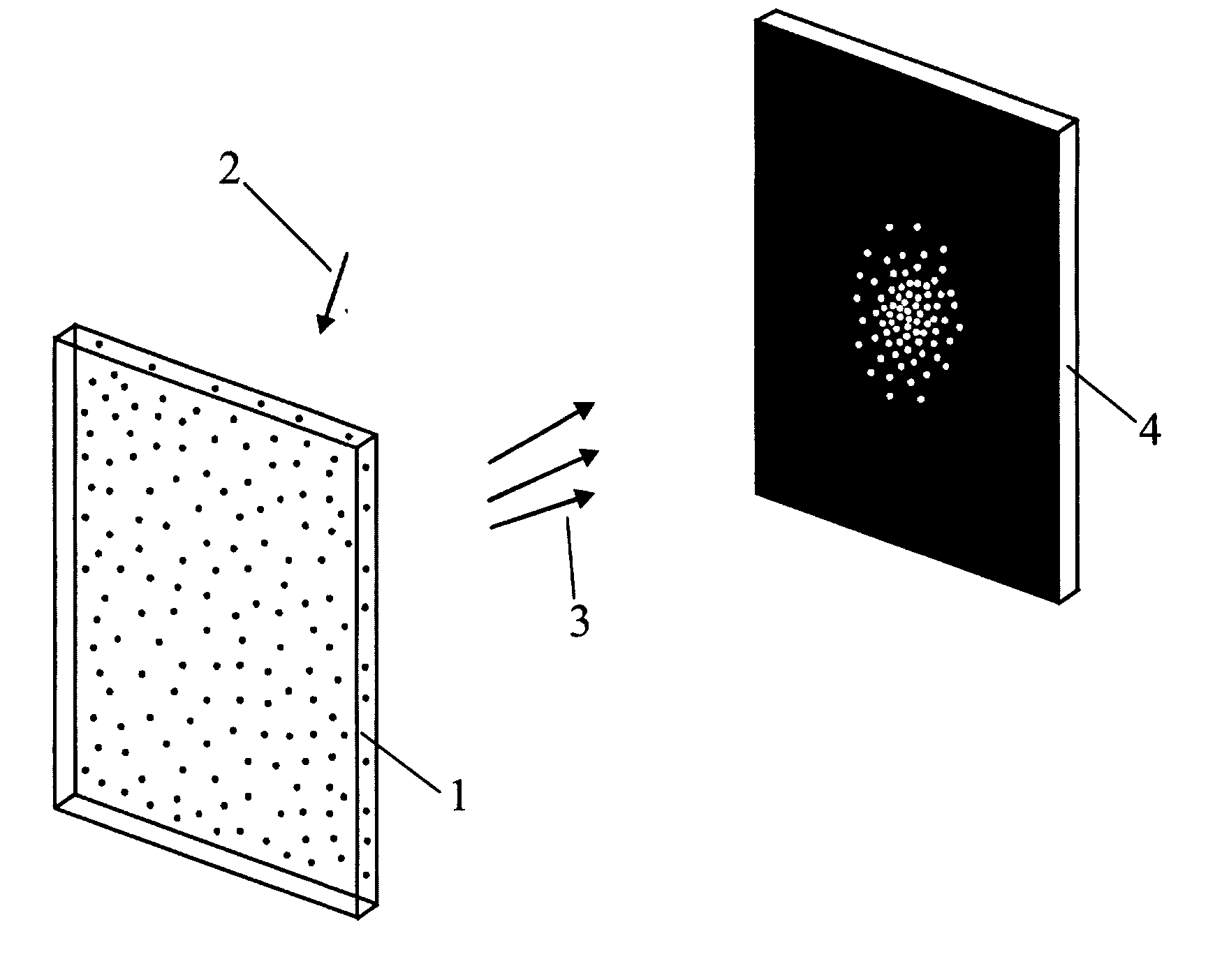
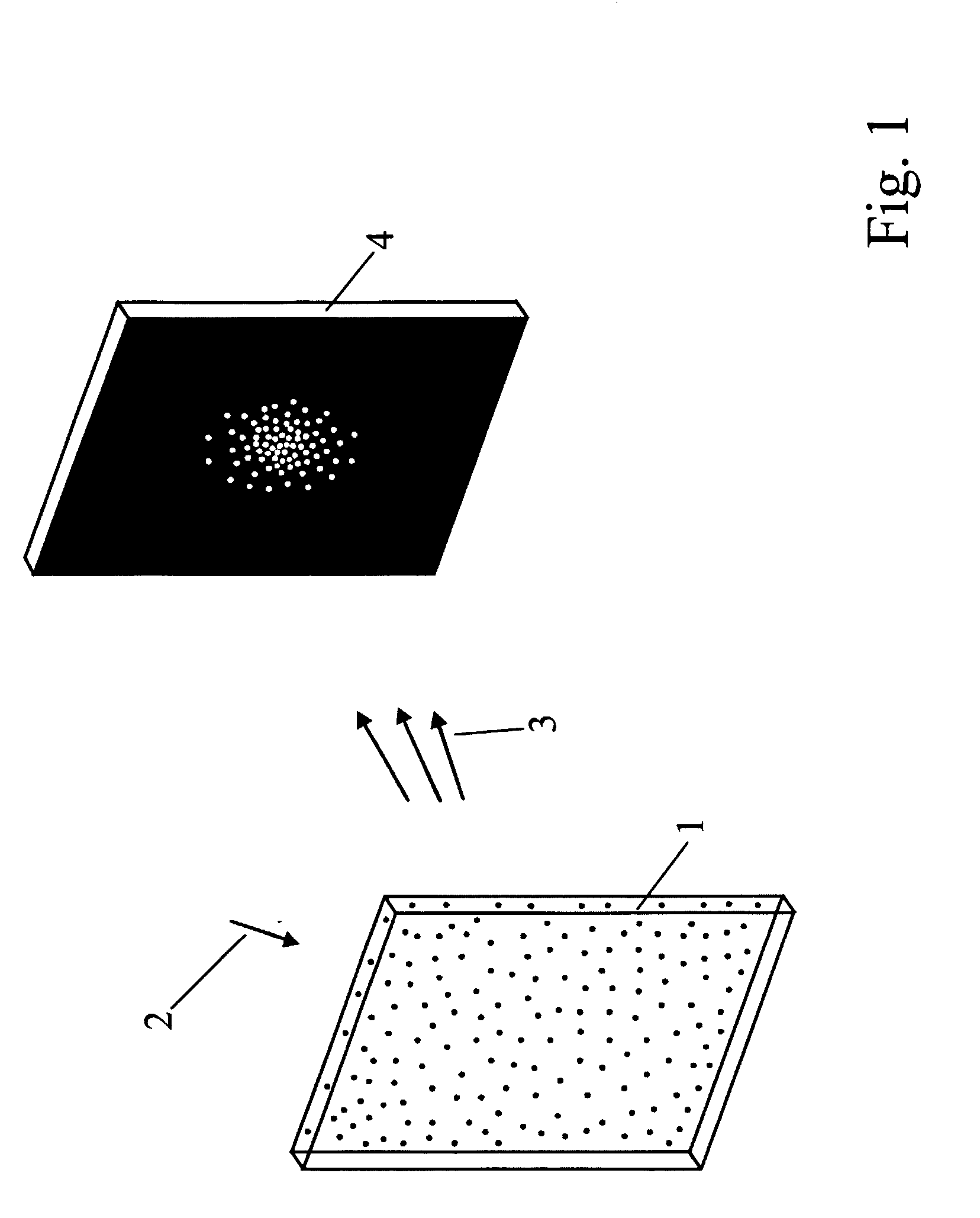
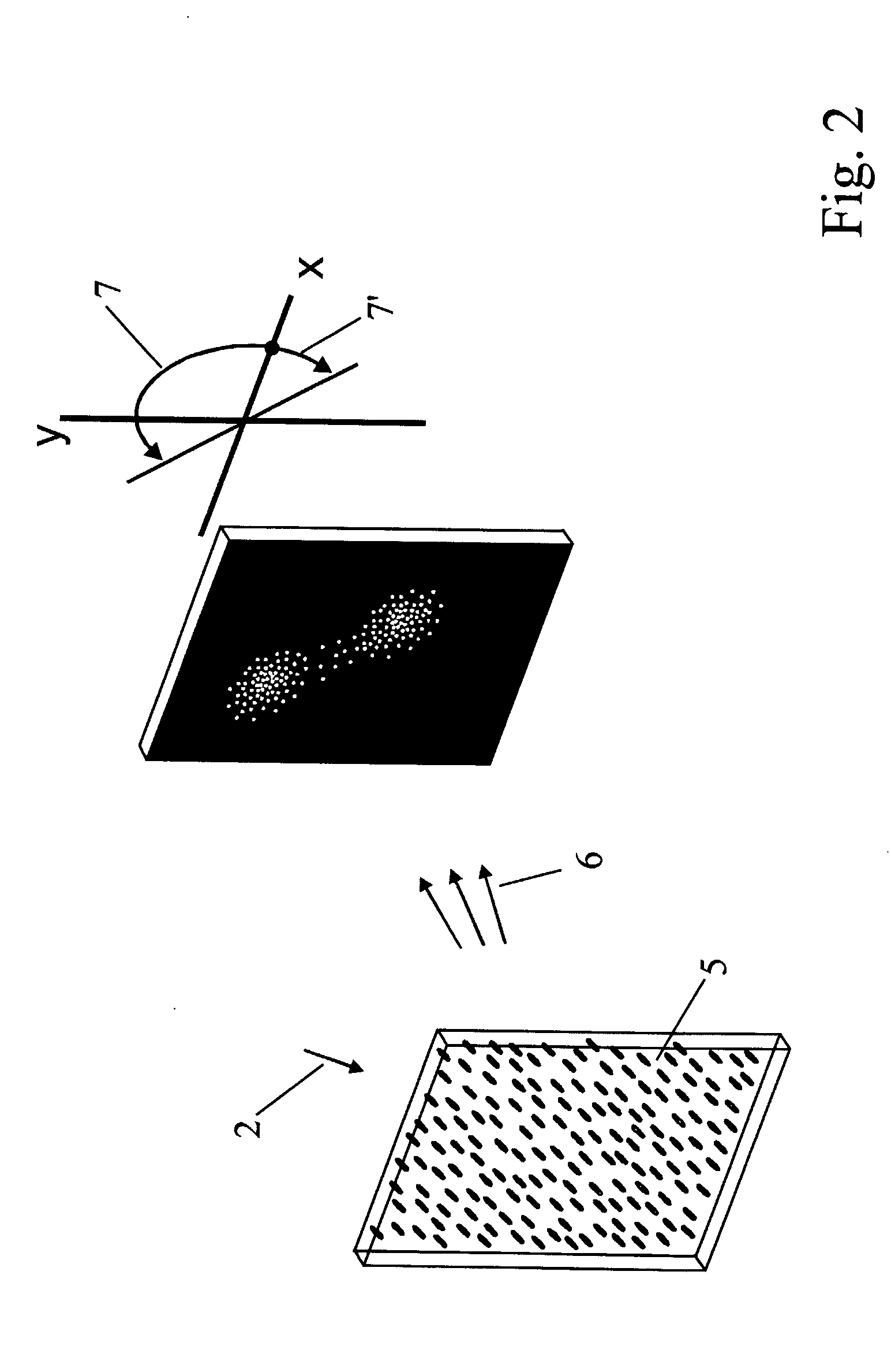
[0098] For all listed examples, which will be described in more detail, anisotropic scattering patterns according to FIG. 15 have been used (two differing anisotropy orientations). With the use of one patterned chromium mask, security devices with graphical illustrations, rastered grey scales and high resolution images (pictures) have been obtained. The pixel size is around 20 micrometers but could be made larger as well as even smaller (<10 micrometers).
example 1
[0099] A first example has been fabricated according to FIG. 3. As interference layer 11, a specially made three-layer Fabry-Perot reflector or an interference filter commercially available from Edmund Industrial Optics with a red reflection was used. Onto the interference layer 11 an anisotropic scattering film 10 was coated according to the film preparation described in WO-A-01 / 29148. As a photoalignment material, the material ROP103 from Rolic Technologies was used and coated with a film thickness of 30 to 60 nanometers by spin coating or by kbar coating. This film was exposed to UV light of a mercury vapor lamp of 1000 Watt in a Karl Suess housing and delivering about 3 mW / cm2 of 305 nm linearly polarised UV light. The UV light was polarised with a Moxtek (US) linear polariser. The first UV exposure also involved a masking of the photoalignment layer with a patterned chromium mask. The first exposure with linearly polarised UV light was carried out at with azimuthal orientation ...
example 2
[0103] A second example has been fabricated according to FIG. 6. In this case the anisotropic scattering film 10 is part of the interference film and therefore partly metallised 14. In a first step, a substrate 12 was metallised with aluminum by DC sputtering leading to the layer 9. The sputtering took place at an Argon flow of about 80 ml / min and a DC power of 300 W. The sample had a distance of 90 mm from the aluminum sputter target. The exposure time was 120 s. It resulted a highly reflecting aluminum film 9 for the visible wavelength range.
[0104] Then, a thin-film of a crosslinkable material was coated onto the metal reflector. In the present case a 15% diacrylate solution of butandiol-diacrylate (BDDA) in cyclopentanone was used. The solution was doped with 1% of BHT (Butylated Hydroxytoluene, also called 2,6,-di-(t-butyl)-4-hydroxytoluene) and 1% of the photoinitator Irgacure 369 of Ciba SC (CH). Again the film can be deposited by spin coating or kbar coating. The thickness o...
PUM
 Abstract
Description
Claims
Application Information