Flip-Chip Device Having Underfill in Controlled Gap

Inactive Publication Date: 2007-08-30
TEXAS INSTR INC
View PDF7 Cites 125 Cited by
  • Summary
  • Abstract
  • Description
  • Claims
  • Application Information

AI Technical Summary

Benefits of technology

[0007] Applicant recognizes the need for an assembly methodology, which, on one hand, can accept the shrinking ball diameter and ball pitch of flip-chip devices, yet on the other hand decouples the width of the gap in assembled devices from the ball diameter so that the polymer material can fill the gap uniformly without leaving voids. The stress-di

Problems solved by technology

These stresses tend to fatigue the joints and the bumps, resulting in cracks and eventual failure of the assembly.
It is well known in the industry that the temperature cycling needed for the underfill curing process can create thermomechanical stress on its own, which may be detrimental to the chip and/or the solder interconnections.
The stress created by these process

Method used


Image

  • Flip-Chip Device Having Underfill in Controlled Gap
  • Flip-Chip Device Having Underfill in Controlled Gap
  • Flip-Chip Device Having Underfill in Controlled Gap

Examples


Embodiment Construction

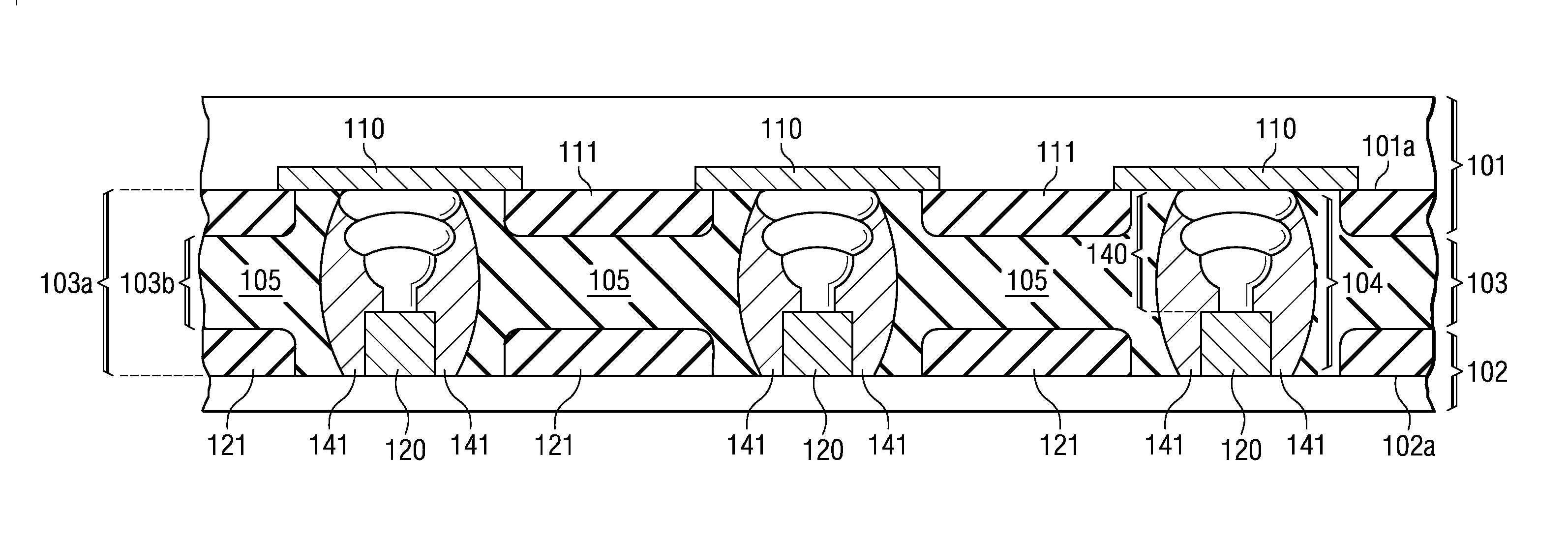
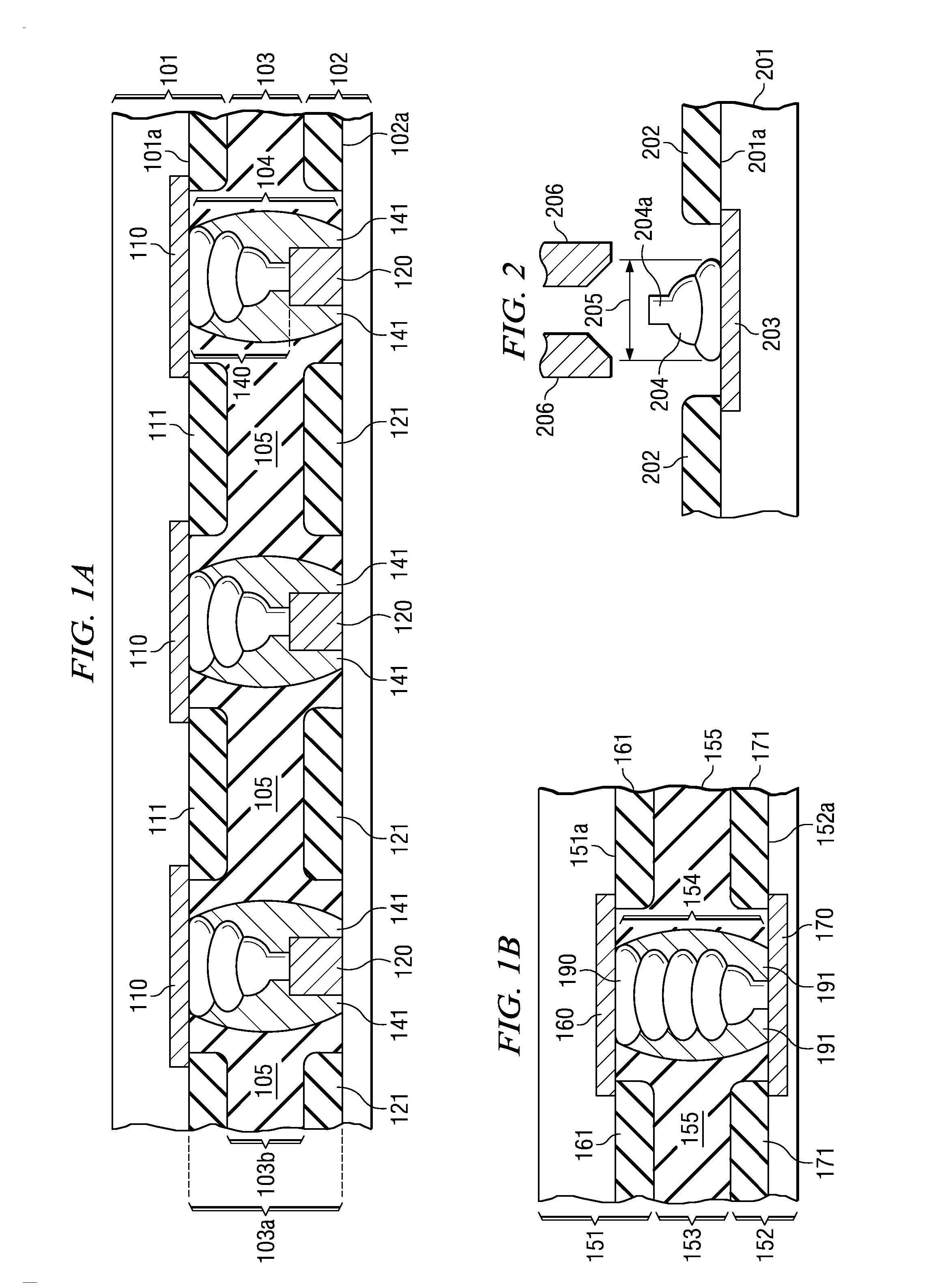
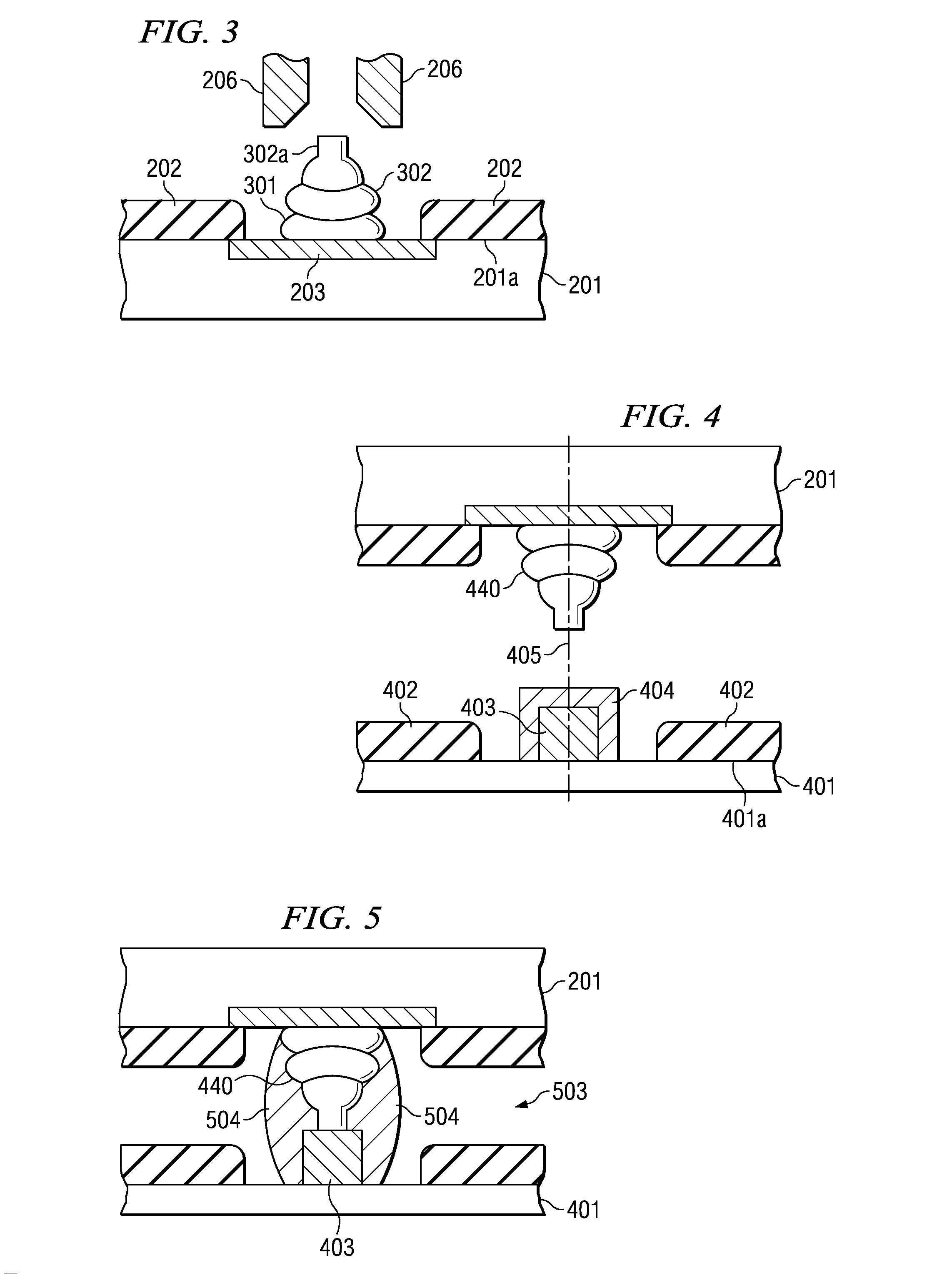
[0021]FIGS. 1A and 1B illustrate portions of assembled semiconductor devices. The device in FIG. 1A includes a semiconductor chip 101 spaced from a workpiece 102 by a gap 103, and a connector 104 bridging the gap and electrically connecting the chip and the workpiece. Gap 103 may be filled with a polymer material 105. The device in FIG. 1B includes a semiconductor chip 151 spaced from a workpiece 152 by a gap 153, and a connector 154 bridging the gap an electrically connecting the chip and the workpiece. Gap 153 may be filled with a polymer material 155.

[0022] Semiconductor chips 101 and 151 are made of a semiconductor material (such as silicon, silicon germanium, or gallium arsenide) and have an active surface (101a, 151a), which is preferably covered by one or more layers of an overcoat (111, 161) such as silicon nitride or silicon oxynitride for mechanical and moisture protection. Overcoat thicknesses range preferably between about 20 and 30 μm, but may be thinner. Windows in th...


PUM


Abstract

A flip-chip and underfilled device, which includes a semiconductor chip (101) with contact pads and a workpiece (102) with contact pads in matching locations; the workpiece may be an insulating substrate or another semiconductor chip. The workpiece and the chip are spaced by a gap (103) of substantially uniform average width. Attached to each chip contact pad is a column-shaped spacer (140), which includes two or more deformed spheres of non-reflow metals, preferably gold, bonded together to a height about equal to the gap width. The spacer is attached to the contact pad (110) substantially normal to the chip surface and extends from the chip pad to the matching workpiece pad (120); it is bonded to the workpiece pad by reflow metals (141) such as tin or tin alloy, which covers at least portions of the workpiece pad and the spacer. The gap may be filled with a polymer material (105) surrounding the reflow metal and spacers.

Description

FIELD OF THE INVENTION [0001] The present invention is related in general to the field of semiconductor devices and processes, and more specifically to low profile flip-chip assembled devices, which provide a controllable gap between chip and substrate for uniform underfilling. DESCRIPTION OF THE RELATED ART [0002] When an integrated circuit (IC) chip is assembled on an insulating substrate with conducting lines, such as a printed circuit motherboard, by solder bump connections, the chip is spaced apart from the substrate by a gap; the solder bump interconnections extend across the gap. The IC chip is typically a semiconductor such as silicon, silicon germanium, or gallium arsenide, the substrate is usually made of ceramic or polymer-based materials such as FR-4. Consequently, there is a significant difference between the coefficients of thermal expansion (CTE) of the chip and the substrate; for instance, with silicon (about 2.5 ppm / ° C.) as the semiconductor material and plastic FR...

Claims


Application Information

Patent Timeline
IPC IPC(8): H01L23/48
CPCH01L21/563H01L2924/10253H01L24/11H01L24/12H01L24/16H01L24/28H01L24/81H01L25/0657H01L25/50H01L2224/1134H01L2224/13021H01L2224/1308H01L2224/13144H01L2224/13147H01L2224/16225H01L2224/73203H01L2224/81136H01L2224/81193H01L2224/8121H01L2224/81815H01L2224/83102H01L2224/83855H01L2224/92125H01L2225/06513H01L2924/01013H01L2924/01015H01L2924/01029H01L2924/01032H01L2924/01046H01L2924/01047H01L2924/0105H01L2924/01079H01L2924/01082H01L2924/12044H01L2924/14H01L23/49811H01L2224/73204H01L2224/32225H01L2224/136H01L2924/00013H01L2924/01006H01L2924/01023H01L2924/01033H01L2924/01087H01L2924/014H01L2924/00014H01L2224/13099H01L2924/00H01L2924/3512H01L2924/15787H01L2924/181H01L2224/05567H01L2224/05573H01L2224/05624H01L2224/05647H01L24/05
Inventor GERBER, MARK A.KADOGUCHI, SOHICHIHAKUNO, MASAKAZU
Owner TEXAS INSTR INC
Why Eureka
Try Eureka