Method for rapid printing of near-field and imprint lithographic features

a technology of lithographic features and near-field, which is applied in the field of material processing systems, can solve the problems of limiting the ability to produce extremely small structural features for integrated circuits, many problems that must be overcome, and it is not possible to print an entire wafer at once, so as to achieve high throughput and improve the effect of throughput and resolution

Inactive Publication Date: 2007-08-30
MICRON TECH INC
View PDF57 Cites 97 Cited by
  • Summary
  • Abstract
  • Description
  • Claims
  • Application Information

AI Technical Summary

Benefits of technology

[0021] Using the present system, two or more heads, each with its own template can be used simultaneously on a single wafer or other substrate. The present apparatus and methods for printing multiple fields on a substrate in parallel advantageously provide increased throughput by a factor of two or more, according to the number of imprint heads that are employed within a processing unit. For example, in the use of processing unit constructed with four imprint heads, a waf...

Problems solved by technology

This limits the ability to produce extremely small structural features for integrated circuits.
With current imprint and sub-wavelength printing technologies, it is not possible to print an entire wafer at once due to alignment and overlay (registration) problems and image distortion associated with full-size masks and printing a large area.
Imprint and near-field lithography techniques are very promising but have many problems that must ov...

Method used


Image

  • Method for rapid printing of near-field and imprint lithographic features
  • Method for rapid printing of near-field and imprint lithographic features
  • Method for rapid printing of near-field and imprint lithographic features

Examples


Embodiment Construction

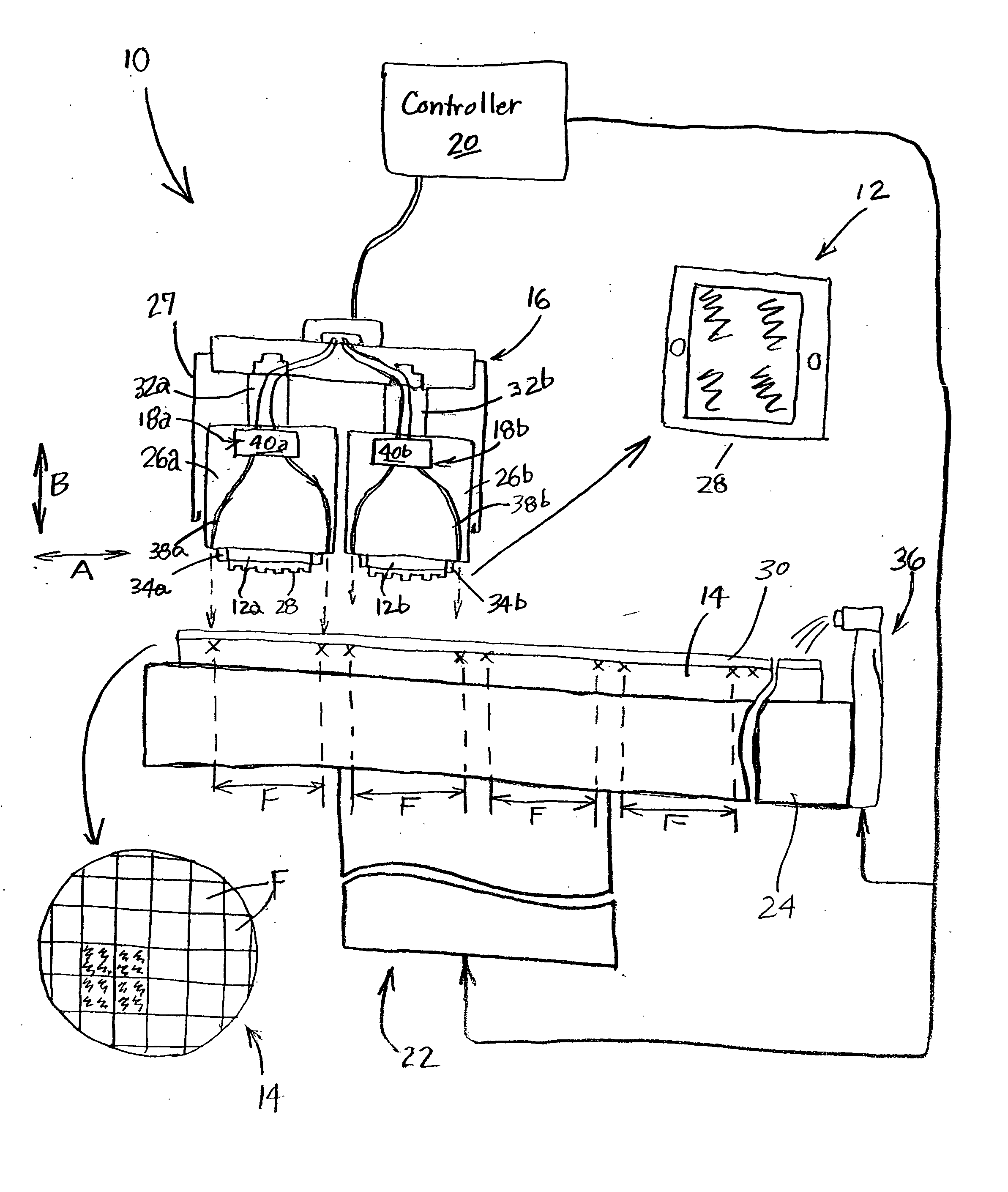
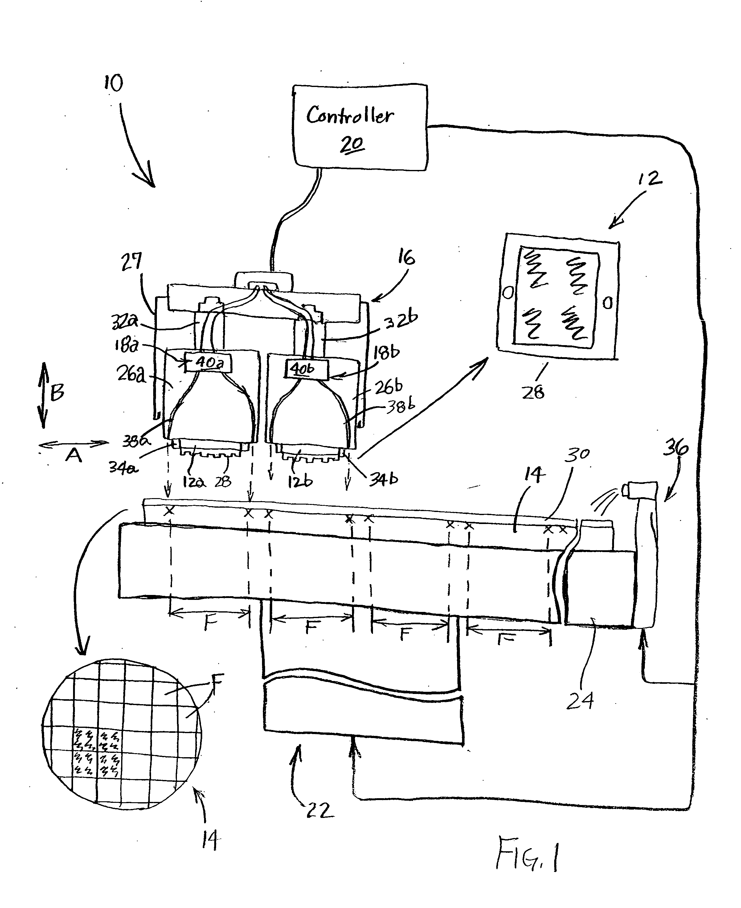
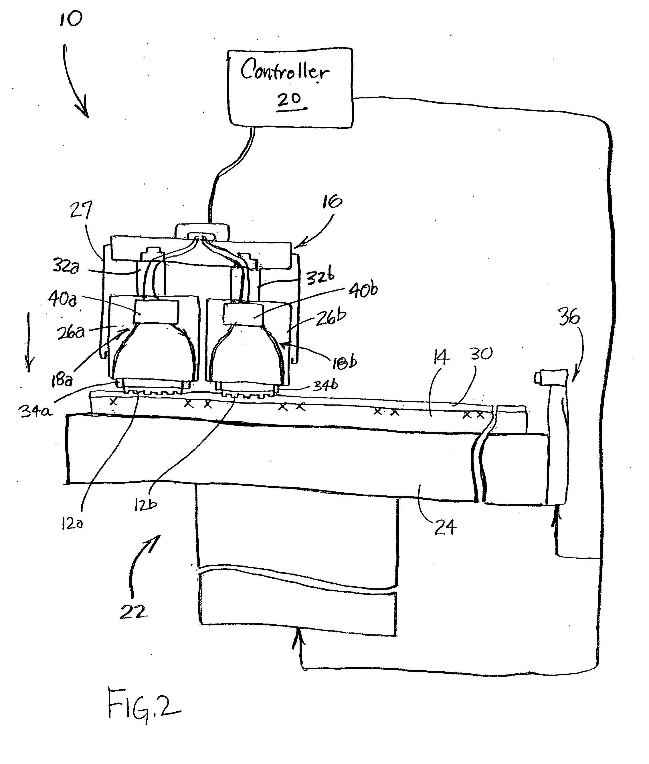
[0029] The following description with reference to the figures provides illustrative examples of lithography systems for processing multiple locations (fields) on a substrate in parallel. Such description is only for illustrative purposes and it is to be understood that the invention can have application to other apparatus, processes, and technologies. Thus, the present invention is not limited to the described illustrative examples.

[0030] For the convenience of drawings and explanation, the lithographic head unit is shown as having four heads. Other configurations such as a unit having two heads, three heads, or more than four heads, are within the scope of the invention.

[0031] In the context of the current application, the term “semiconductor substrate” or “semiconductive substrate” or “semiconductive wafer fragment” or “wafer fragment” or “wafer” will be understood to mean any construction comprising semiconductor material, including but not limited to bulk semiconductive mater...


PUM

PropertyMeasurementUnit
Lightaaaaaaaaaa
Surface plasmonaaaaaaaaaa

Abstract

An apparatus, systems, and methods to print multiple fields on a substrate in parallel are provided. The apparatus incorporates a lithographic apparatus composed of two or more lithographic heads coupled to a common housing as a unit, with each head configured to hold a patterned template. Software can be utilized to keep track of what is printed at any given step, and conventional servometers can be used to reposition the head unit and templates in multiple steps to print the remainder of a wafer.

Description

FIELD OF THE INVENTION [0001] The invention relates generally to material processing systems, and more particularly to lithography systems. BACKGROUND OF THE INVENTION [0002] Lithography is a key process in the fabrication of semiconductor integrated circuits. Photolithography typically involves projecting an image through a reticle or mask onto a thin film of photoresist or other material that covers a semiconductor wafer or other substrate, and developing the film to remove exposed or unexposed portion s of the resist to produce a pattern in subsequent processing steps. [0003] In semiconductor processing, the continual shrink in feature sizes requires systems to produce smaller features. However, with conventional photolithography using light, the minimum feature size and spacing between patterns is generally on the order of the wavelength of the radiation used to expose the film layer. This limits the ability to produce extremely small structural features for integrated circuits....

Claims


Application Information

Patent Timeline
IPC IPC(8): B29C59/02
CPCB82Y10/00B82Y40/00G03F7/0002G03F9/7042G03F9/703G03F9/7038G03F7/7035
Inventor MACKEY, JEFFSANDHU, GURTEJ
Owner MICRON TECH INC
Why Eureka
Try Eureka