Polymer microcavity and microchannel devices and fabrication method

a technology of microchannels and polymers, applied in the manufacture of electrode systems, cold cathode manufacturing, electric discharge tubes/lamps, etc., can solve the problems of short lifetime of microplasma devices, and difficult to manufacture small sizes

Active Publication Date: 2007-08-30
THE BOARD OF TRUSTEES OF THE UNIV OF ILLINOIS
View PDF36 Cites 34 Cited by
  • Summary
  • Abstract
  • Description
  • Claims
  • Application Information

AI Technical Summary

Problems solved by technology
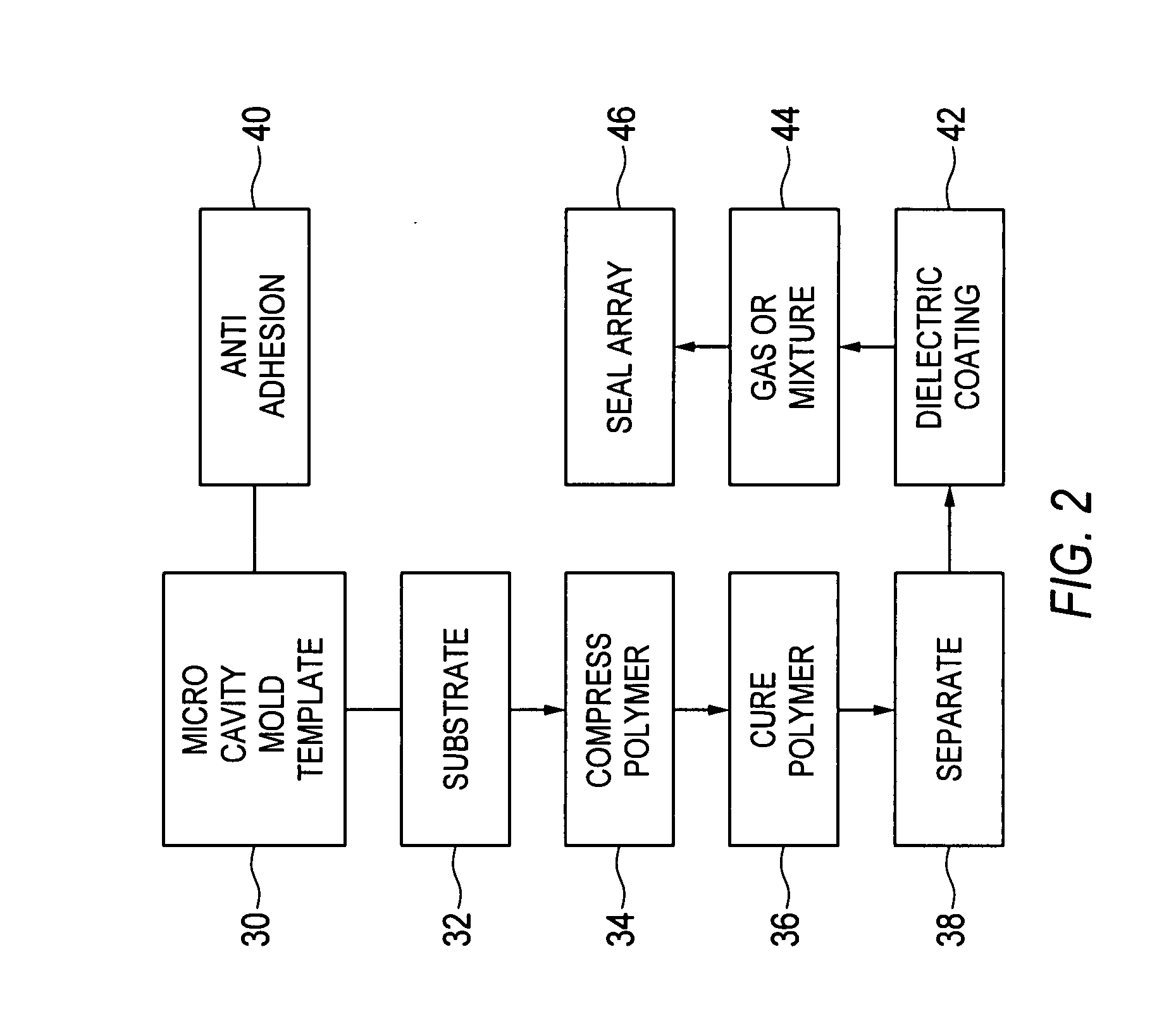
Early microplasma devices were driven by direct current (DC) voltages and exhibited short lifetimes for several reasons, including sputtering damage to the metal electrodes.
For example, with laser ablation and mechanical drilling, the size of the microcavity is typically limited to about 50 μm, with smaller sizes more difficult to make.
Additionally, the cross-sections of microcavities formed by ablation and drilling methods are not completely uniform.
In the case of drilling, mechanical wear of drill bits and mechanical tolerances prevent the achievement of accurate dimensional control and repeatability.
Also, the serial nature of the cavity drilling procedure makes the time and cost of processing prohibitive for the production of large arrays of microcavity plasma devices.
Another drawback is that the techniques used for microcavity formation are not readily adaptable to produce other features, e.g., channels.
While representing an important step in the development of microdischarge devices, micromachined fabrication approaches also have limitations.
One limitation is that the size of an individual array is limited to the size of the silicon substrate.
Second, the cost of a device is determined not only by the substrate cost, but also by the cost of performing an expensive series of photolithographic, thin film deposition, and etching steps on each wafer in the batch.
Finally, although silicon wafers are a convenient substrate due to the wide range of processing options that are available, silicon is an optically opaque material, and is therefore not suitable for applications such as heads-up displays or applications requiring lateral propagation or coupling of visible light between microcavity plasma devices in an array.
Array cost is dominated by the cost of performing multiple photolithography steps.
Current flat panel display solutions suffer from a number of drawbacks.
Consequently, PDPs must be sealed hermetically within an enclosure (normally, glass) that is sufficiently robust (i.e., thick) to withstand atmospheric pressure and this factor is primarily responsible for the undesirably large weight of these displays.
Practical designs that would permit the use of microcavity plasma devices would likely alter the landscape of the flat panel display industry.

Method used


Image

  • Polymer microcavity and microchannel devices and fabrication method
  • Polymer microcavity and microchannel devices and fabrication method
  • Polymer microcavity and microchannel devices and fabrication method

Examples


Embodiment Construction

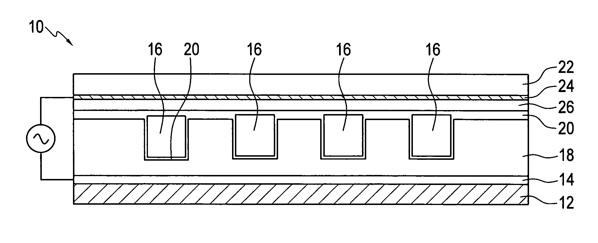
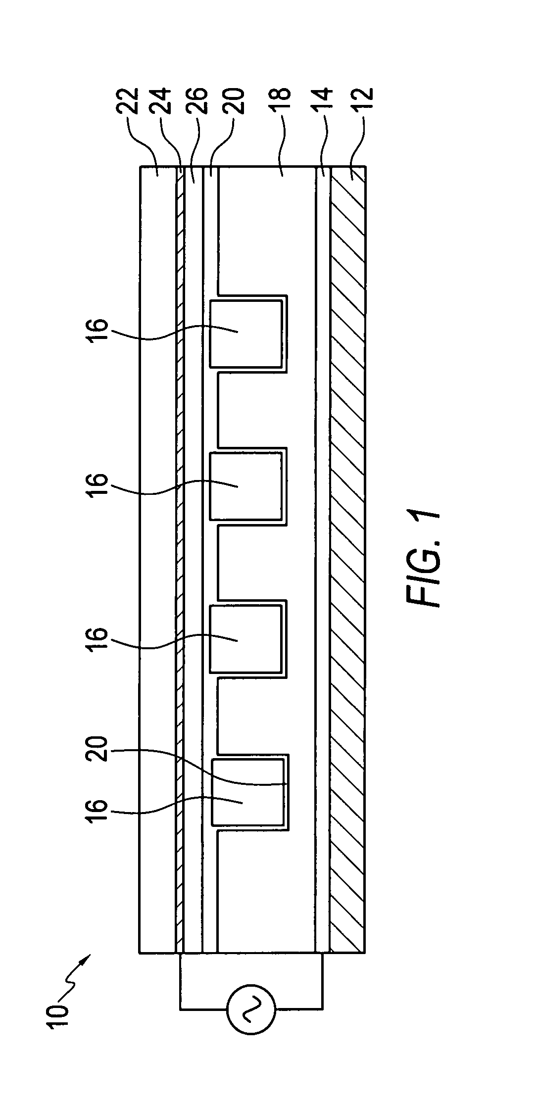
[0029] Microcavity plasma device arrays of different embodiments of the invention provide polymer microcavities that are readily mass fabricated, can be transparent, and can be rigid or flexible. A preferred embodiment of the invention is a polymer microcavity plasma array formed on a substrate. In a preferred embodiment, the polymer is a transparent polymer having transparency in a particular range of interest, e.g., such as infrared (IR), visible, ultraviolet (UV) or a range extending to portions of the IR, visible and UV ranges. In preferred embodiments, the transparent polymer is transparent in at least a portion of the visible range. The substrate and electrodes can also be transparent in preferred embodiments. In preferred embodiments, transparent polymer microcavities are formed in a flexible polymer material. In other preferred embodiments, the transparent polymer microcavities are formed in a rigid polymer material. Arrays of the invention can be very large format, as array...


PUM

PropertyMeasurementUnit
diameteraaaaaaaaaa
sizeaaaaaaaaaa
areaaaaaaaaaaa

Abstract

A microplasma device includes a substrate and either or both of a microchannel or microcavity defined in a polymer layer supported by the substrate. Electrodes arranged with respect to the polymer material can excite a plasma in a discharge medium contained in the microchannel or the microcavity or both. A method of forming a microplasma device places a curable polymer material between a mold having a negative volume impression of microcavities and / or microchannels and a substrate. The polymer is cured and then the mold is separated from the solid polymer.

Description

PRIORITY CLAIM [0001] This application claims priority under 35 U.S.C. §119 from co-pending provisional application Ser. No. 60 / 761,316, filed Jan. 23, 2006.STATEMENT OF GOVERNMENT INTEREST [0002] This invention was made with government support under contract number F49620-03-1-0391 awarded by the Air Force Office of Scientific Research (AFOSR). The government has certain rights in this application.FIELD OF THE INVENTION [0003] The present invention relates to microcavity plasma devices, also known as microdischarge or microplasma devices. BACKGROUND [0004] Microcavity plasmas, plasmas confined to a cavity with a characteristic spatial dimension <1 mm, have several distinct advantages over conventional, macroscopic discharges. For example, the small physical dimensions of microcavity plasma devices allow them to operate at gas or vapor pressures much higher than those accessible to a macroscopic discharge such as that produced in a fluorescent lamp. When the diameter of the micro...

Claims


Application Information

Patent Timeline
Patent Type & Authority Applications(United States)
IPC IPC(8): H01J17/49H01J17/16
CPCH01J9/245H01J11/18B29C65/70B29C35/02H01J65/046H05H1/2406
Inventor EDEN, J. GARYPARK, SUNG-JINLU, MENGCUNNINGHAM
Owner THE BOARD OF TRUSTEES OF THE UNIV OF ILLINOIS
Why Eureka
Try Eureka