Semiconductor integrated circuit device and power source wiring method therefor

Inactive Publication Date: 2007-09-13
PANASONIC SEMICON SOLUTIONS CO LTD
View PDF7 Cites 7 Cited by
  • Summary
  • Abstract
  • Description
  • Claims
  • Application Information

AI Technical Summary

Benefits of technology

[0012]The present invention has been achieved in view of the problem mentioned above and it is therefore an object of the present invention to

Problems solved by technology

Thus, when the width of the signal line has been reduced and the amount of the current has increased, the density of a current in wiring in the semiconductor integrated circuit device has increased so that a break in wiring and a short circuit therein due to electromigration have caused problems.
When the clock skew is large, it may cause a reduction in operating frequency and even the misoperation of a circuit.
Even in such a clock tree with equal wiring lengths, when wiring capacitances are different under the influence of surrounding wiring lines or the gate capacitances of cells driven by the relay buffers are different, the clock skew undesirably occurs depending on a delay in the clock tree portion.
Because the relay buffers drive a large number of flip-flops and long wiring lines in the clock tree, a load to be driven

Method used


Image

  • Semiconductor integrated circuit device and power source wiring method therefor
  • Semiconductor integrated circuit device and power source wiring method therefor
  • Semiconductor integrated circuit device and power source wiring method therefor

Examples


Example

Embodiment 1

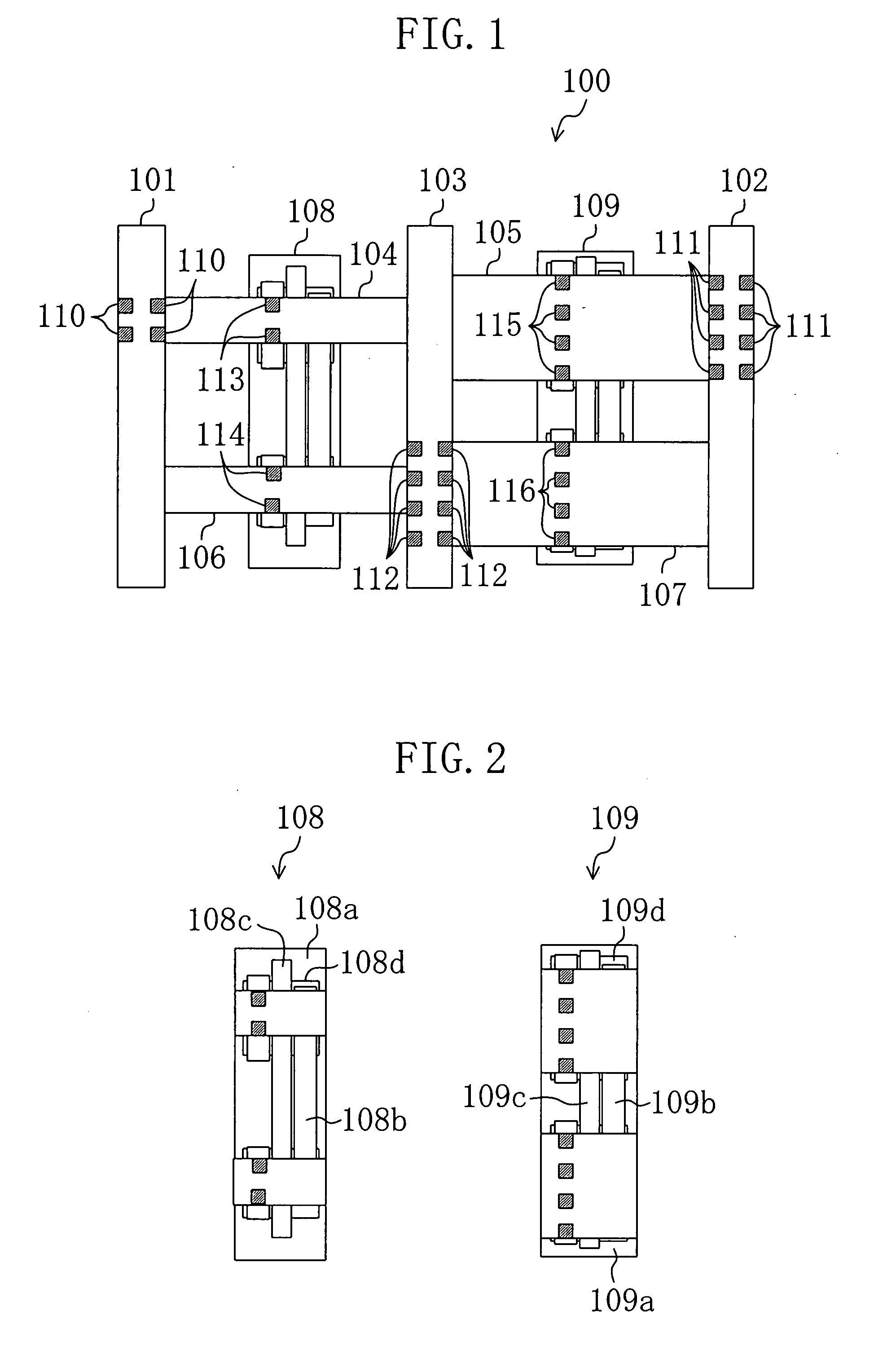
[0023]FIG. 1 is a layout diagram showing a structure of a semiconductor integrated circuit device 100 according to the first embodiment of the present invention. As shown in the drawing, the semiconductor integrated circuit device 100 comprises: a first power source strap 101; a second power source strap 102; a third power source strap 103; a first cell power source line 104; a second cell power source line 105; a third cell power source line 106; a fourth cell power source line 107; a first standard cell 108, a second standard cell 109; and contacts 110 to 116. First, a description will be given to the positional relations among the individual components placed in the semiconductor integrated circuit device 100 and the like.

[0024]The first, second, and third power source straps 101, 102, and 103 are placed in the same wiring layer.

[0025]The first and second power source straps 101 and 102 are power source lines each for supplying a first potential (e.g., VDD). The first...

Example

Embodiment 2

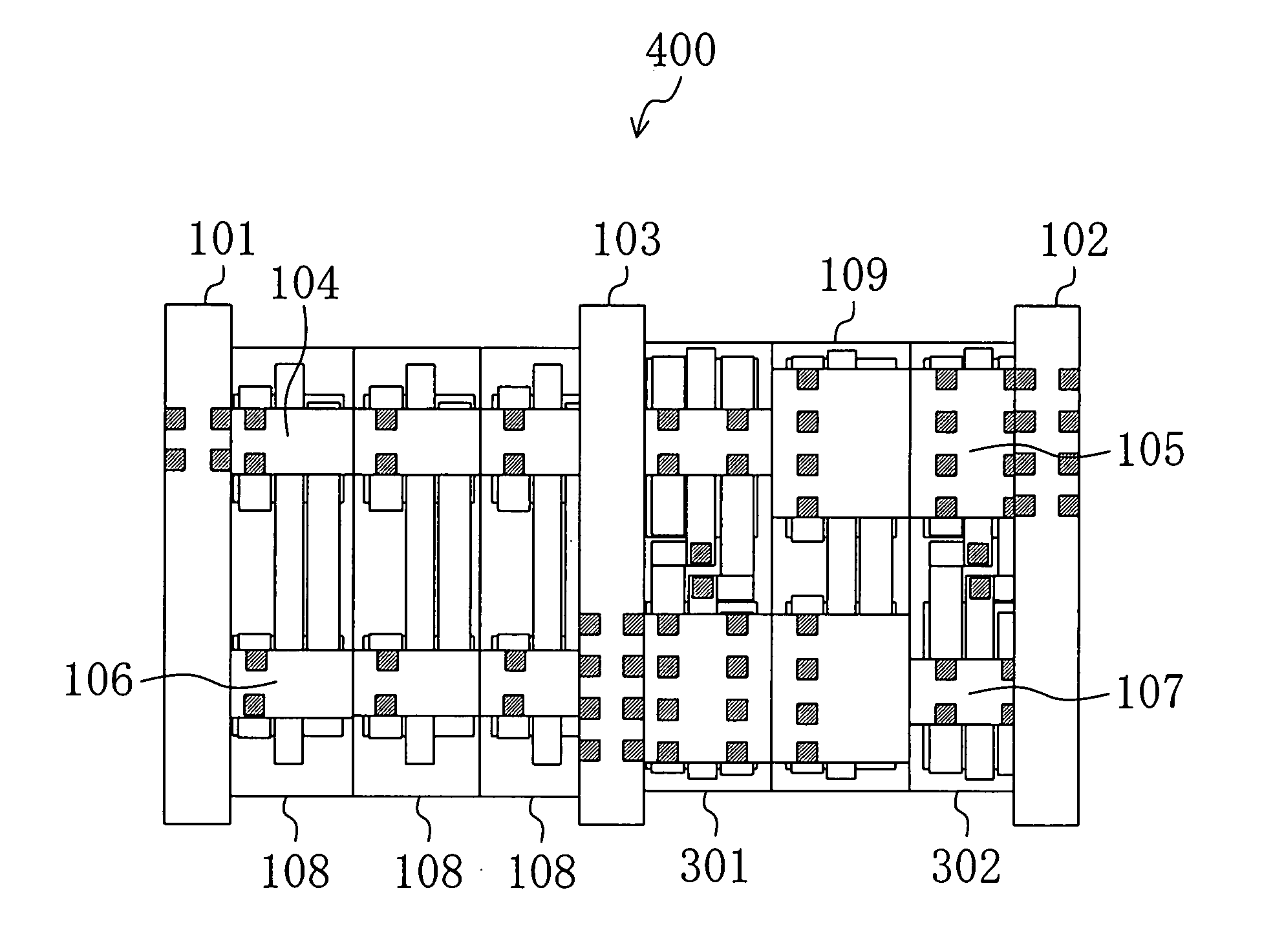
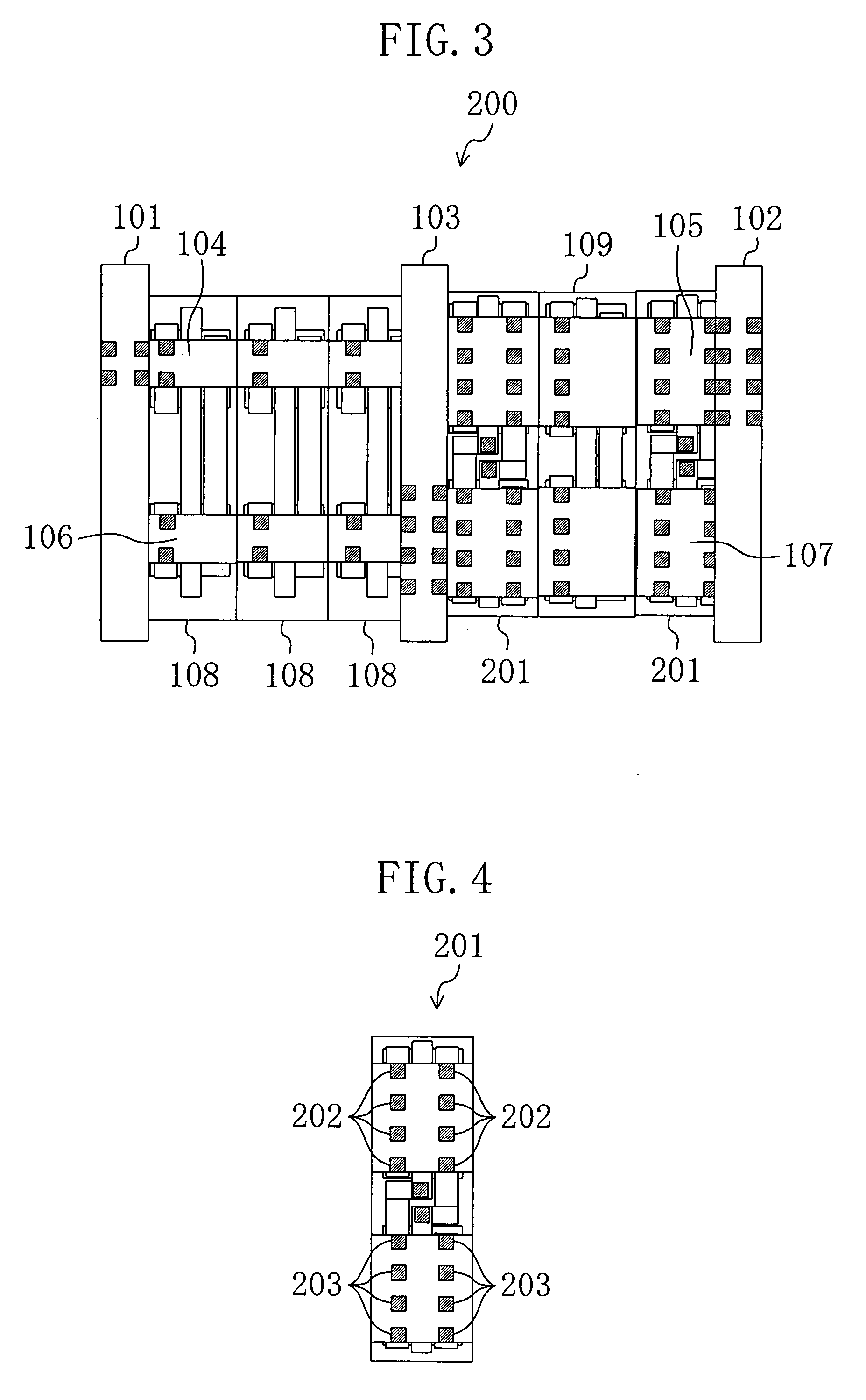
[0046]FIG. 3 is a layout diagram showing a structure of a semiconductor integrated circuit device 200 according to the second embodiment of the present invention. As shown in the drawing, the semiconductor integrated circuit device 200 comprises: the first power source strap 101; the second power source strap 102; the third power source strap 103, the first cell power source line 104; the second cell power source line 105; the third cell power source line 106; the fourth cell power source line 107; the first standard cells 108; the second standard cell 109; the contacts 110 to 116; and decoupling capacitor cells 201.

[0047]Each of the decoupling capacitor cells 201 is a standard cell comprising a decoupling capacitor in which a capacitance is formed by using a gate oxide film. The decoupling capacitor cells 201 are connected to the second cell power source line 105 via contacts 202 and also connected to the fourth cell power source line 107 via contacts 203. As a result, ...

Example

[0059]In the third embodiment, a description will be given to an example of a semiconductor integrated circuit device in which a large region can be provided for other signal lines. The semiconductor integrated circuit device according to the third embodiment is different from the semiconductor integrated circuit device 200 in that decoupling capacitor cells 301 or decoupling capacitor cells 302 (see FIG. 5), instead of the decoupling capacitor cells 201, are placed in the vacant space between the power source straps between which the second standard cell 109 is placed.

[0060]Each of the decoupling capacitor cells 301 and 302 is a standard cell comprising a decoupling capacitor in which a capacitance is formed by using a gate oxide film. As shown in FIG. 5, in the decoupling capacitor cell 301, one of cell power source lines is wider than the other of the cell power source lines. Specifically, the wider cell power source line has the same width as the cell power source line supplying...


PUM


Abstract

In a semiconductor integrated circuit device, from a first power source strap supplying a potential to a first standard cell receiving a supply of the potential, the potential is supplied via a first cell power source line having a constant width. The width of the first cell power source line is determined in accordance with power consumed by the first standard cell and with the number of standard cells that can be placed between the first power source strap and a third power source strap.

Description

BACKGROUND OF THE INVENTION[0001]1. Field of the Invention[0002]The present invention relates to a semiconductor integrated circuit device composed of standard cells arranged therein and to a power source wiring method for the semiconductor integrated circuit device.[0003]2. Description of the Prior Art[0004]In recent years, as digital circuits have become higher in speed and functionality, semiconductor integrated circuit devices have also become increasingly higher in speed and integration degree. To increase the integration degree of a semiconductor integrated circuit device, a fabrication process therefor has been scaled down year after year and, consequently, the width of a signal line used in the semiconductor integrated circuit device has been increasingly reduced. In addition, the increased speed of the semiconductor integrated circuit device has increased an amount of a current flowing in the signal line. Thus, when the width of the signal line has been reduced and the amou...

Claims


Application Information

Patent Timeline
IPC IPC(8): H01L29/00H01L21/00
CPCH01L27/118H01L27/0207
Inventor TSUTSUMI, MASANORI
Owner PANASONIC SEMICON SOLUTIONS CO LTD
Why Eureka
Try Eureka