

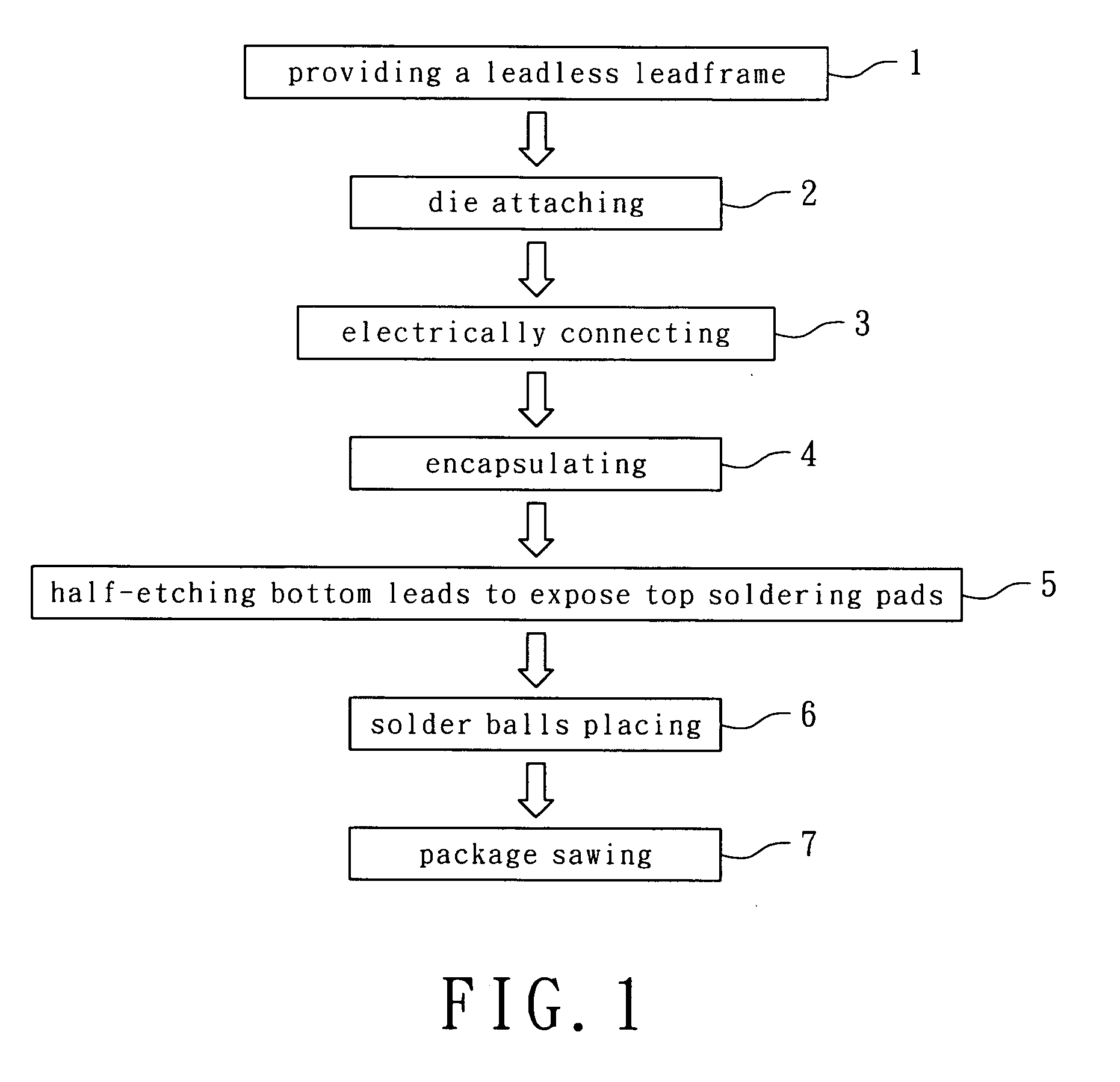
Fabrication processes of leadframe-based BGA packages and leadless leadframe implemented in the processes
a technology of leadframe and process, applied in the direction of electrical apparatus, semiconductor devices, semiconductor/solid-state device details, etc., can solve the problems of mold flash, insufficient height of solder balls or even bridging between, weakening soldering strength, and dropping of solder balls, so as to enhance the adhesion of chip 120, easy detection and removal, and enhance the soldering strength of solder balls
- Summary
- Abstract
- Description
- Claims
- Application Information
AI Technical Summary
Benefits of technology
Problems solved by technology
Method used
Image

Examples
first embodiment
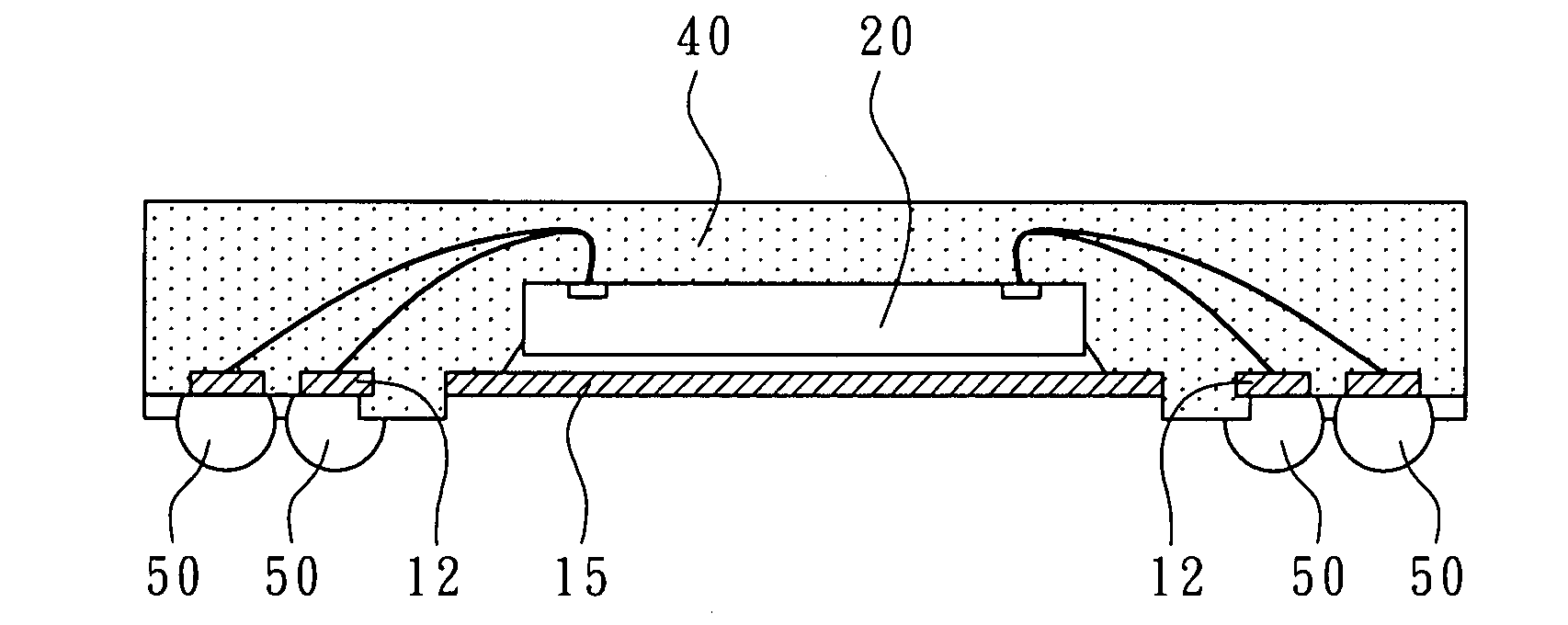
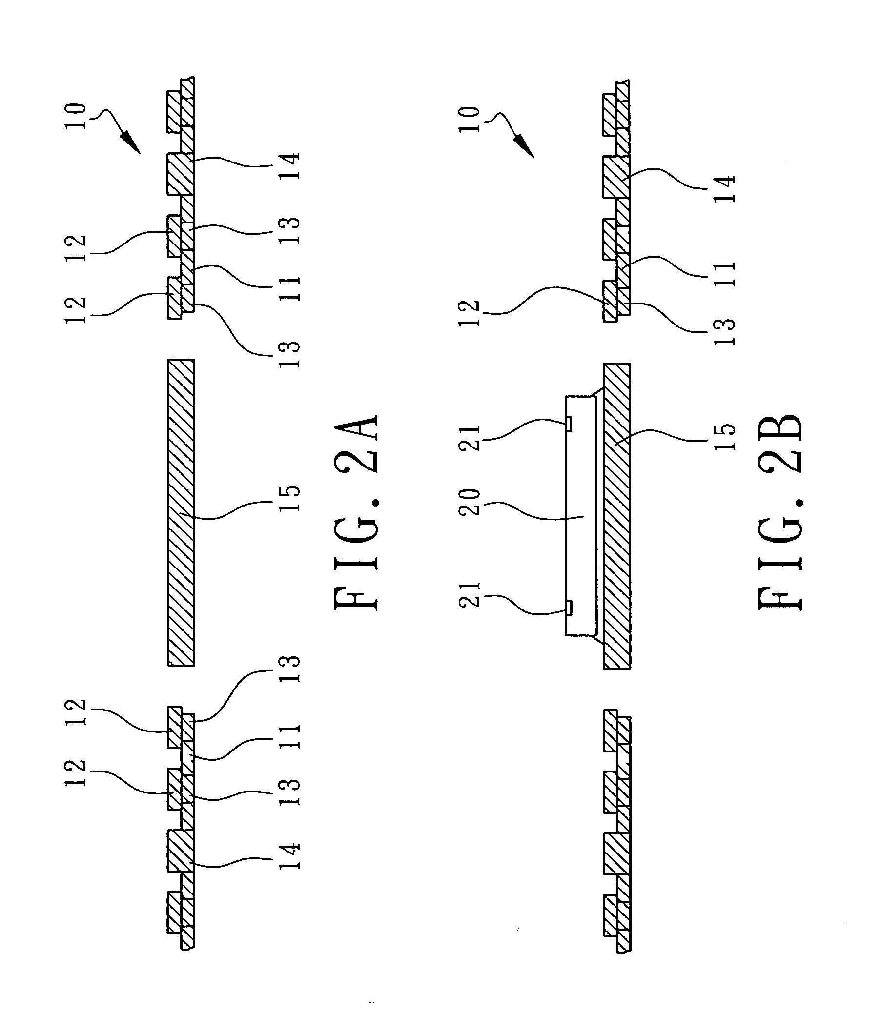
[0017]According to the present invention, firstly, in step 1, as shown in FIG. 2A, a leadless leadframe 10 is provided where a plurality of array packaging units are defined to manufacture a plurality of corresponding leadframe-based BGA packages. As shown in FIGS. 3 and 4, in each packaging unit, the leadless leadframe 10 has a plurality of bottom leads 11 and a plurality of top soldering pads 12. The bottom leads 11 are formed in the lower layer of the leadless leadframe 10. The top soldering pads 12 are formed in the upper layer of the leadless leadframe 10 which are connected with the bottom leads 11. The bottom leads 11 are connected to the frame bars 14 locating at the unit edge of the leadless leadframe 10 to fix the top soldering pads 12. Preferably, as shown in FIG. 3, the top soldering pads 12 are disposed in an array and each of the bottom leads 11 is connected to at least two of the top soldering pads 12 to achieve a high density layout of the top soldering pads 12. As s...
second embodiment
[0025]Another leadframe-based BGA package is revealed in FIG. 5 according to the present invention. The package has a flip-chip configuration, mainly includes a leadless leadframe with top soldering pads 111, a chip 120, an encapsulant 140, and a plurality of solder balls 150. The mainly manufacturing steps are described as shown in FIG. 1. In step 1 of “providing a leadless leadframe”, the leadless leadframe has top soldering pads 111 which are connected by the bottom leads, not shown in the figure. In the present embodiment, the leadless leadframe further has a die pad 112. Then, in the step 2 of “die-attaching”, a chip 120 is flip-chip attached to the leadless leadframe where the active surface 121 of the chip 120 has a plurality of bonding pads 122. By using a plurality of bumps 123 to electrically connect the bonding pads 122 to the top soldering pads 111 to complete step 3 of “electrically connecting” at the same time. Preferably, during die attaching, a die-attaching film 131...
PUM
 Abstract
Description
Claims
Application Information