DRAM with nanofin transistors

a technology of nanofin transistors and drams, which is applied in the direction of nanotechnology, semiconductor devices, electrical apparatus, etc., can solve the problems of difficult formation of shallow junctions, and difficult sub-threshold conduction, so as to minimize drain leakage current, improve dram retention time, and reduce the volume of drain regions

Active Publication Date: 2007-10-04
MICRON TECH INC
View PDF60 Cites 37 Cited by
  • Summary
  • Abstract
  • Description
  • Claims
  • Application Information

AI Technical Summary

Benefits of technology

[0008] Aspects of the present subject matter provide nanofin transistors with near ideal sub-threshold characteristics and miniaturized sub-threshold leakage, and with extremely small drain region volumes to minimize drain leakage currents. One method for fabricating the nanofins involves growing the nanofins on a substrate, using solid phase epitaxial growth to recrystallize amorphous semiconductor on the substrate. Another method for fabricating the nanofins involves etching fins into single crystalline silicon subst

Problems solved by technology

Some product goals include lower power consumption, higher performance, and smaller sizes. FIG. 1 illustrates general trends and relationships for a variety of device parameters with scaling by a factor k. The continuous scaling of MOSFET technology to the deep sub-micron region where channel lengths are less than 0.1 micron (100 nm or 1000 Å) causes significant problems in the conventional transistor structures.
Such shallow junctions are difficult to form by conventional implantation and diffusion techniques.
Sub-threshold conduction is particularly problematic in DRAM tech

Method used


Image

  • DRAM with nanofin transistors
  • DRAM with nanofin transistors
  • DRAM with nanofin transistors

Examples


Embodiment Construction

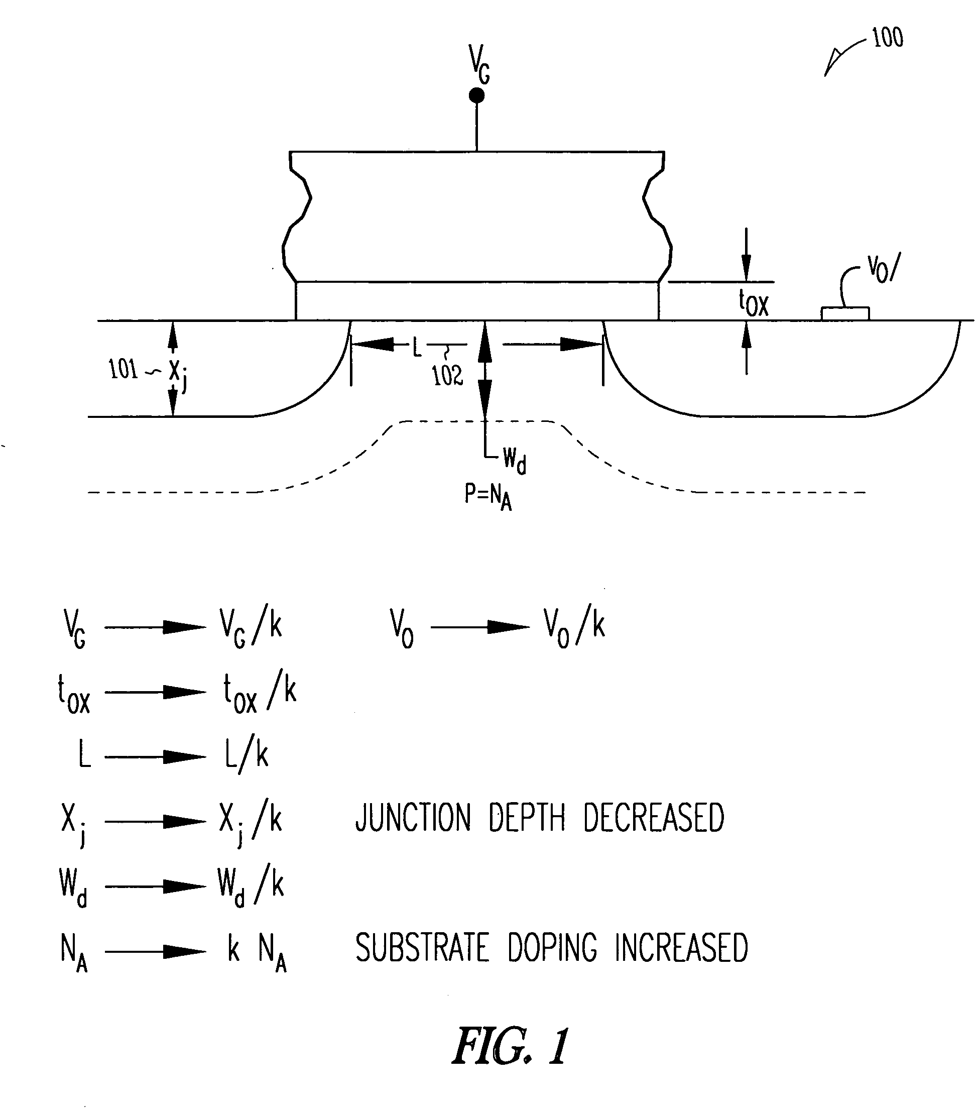
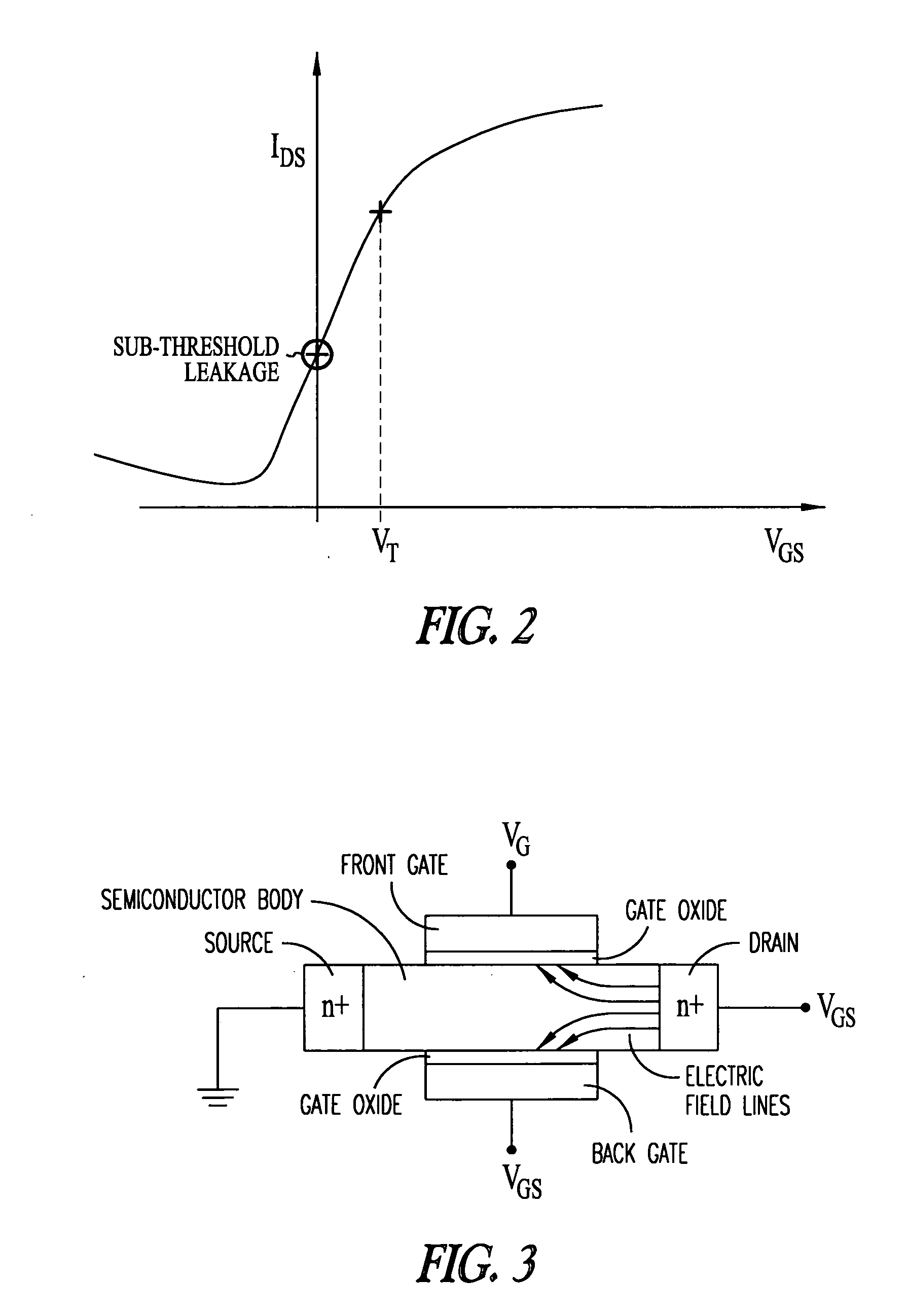
[0028] The following detailed description refers to the accompanying drawings which show, by way of illustration, specific aspects and embodiments in which the present subject matter may be practiced. These embodiments are described in sufficient detail to enable those skilled in the art to practice the present subject matter. The various embodiments of the present subject matter are not necessarily mutually exclusive as aspects of one embodiment can be combined with aspects of another embodiment. Other embodiments may be utilized and structural, logical, and electrical changes may be made without departing from the scope of the present subject matter. In the following description, the terms “wafer” and “substrate” are interchangeably used to refer generally to any structure on which integrated circuits are formed, and also to such structures during various stages of integrated circuit fabrication. Both terms include doped and undoped semiconductors, epitaxial layers of a semiconduc...


PUM


Abstract

One aspect of the present subject matter relates to a memory. A memory embodiment includes a nanofin transistor having a first source/drain region, a second source/drain region above the first source/drain region, and a vertically-oriented channel region between the first and second source/drain regions. The nanofin transistor also has a surrounding gate insulator around the nanofin structure and a surrounding gate surrounding the channel region and separated from the nanofin channel by the surrounding gate insulator. The memory includes a data-bit line connected to the first source/drain region, at least one word line connected to the surrounding gate of the nanofin transistor, and a stacked capacitor above the nanofin transistor and connected between the second source/drain region and a reference potential. Other aspects are provided herein.

Description

CROSS REFERENCE TO RELATED APPLICATIONS [0001] This application is related to the following commonly assigned U.S. patent applications which are filed on even date herewith and are herein incorporated by reference in their entirety: “Nanowire Transistor With Surrounding Gate,” U.S. application Ser. No. ______, filed on ______ (Attorney Docket No. 1303.167US1); “Grown Nanofin Transistors,” U.S. application Ser. No. ______, filed on ______ (Attorney Docket No. 1303.168US1); “Etched Nanofin Transistors,” U.S. application Ser. No. ______, filed on ______ (Attorney Docket No. 1303.170US1); and “Tunneling Transistor With Sublithographic Channel,” U.S. application Ser. No. ______, filed on ______ (Attorney Docket No. 1303.172US1).TECHNICAL FIELD [0002] This disclosure relates generally to semiconductor devices, and more particularly, to DRAMs with nanofin transistors. BACKGROUND [0003] The semiconductor industry has a market driven need to reduce the size of devices, such as transistors, a...

Claims


Application Information

Patent Timeline
IPC IPC(8): H01L29/94
CPCB82Y10/00H01L27/10823H01L27/10826H01L27/10876H01L2029/7858H01L29/785H01L2924/13067H01L21/823487H01L27/10879H10B12/36H10B12/34H10B12/056H10B12/053H01L21/02532H10B12/0335
Inventor FORBES, LEONARD
Owner MICRON TECH INC
Why Eureka
Try Eureka