Composition Control For Photovoltaic Thin Film Manufacturing
- Summary
- Abstract
- Description
- Claims
- Application Information
AI Technical Summary
Benefits of technology
Problems solved by technology
Method used
Image
Examples
example 1
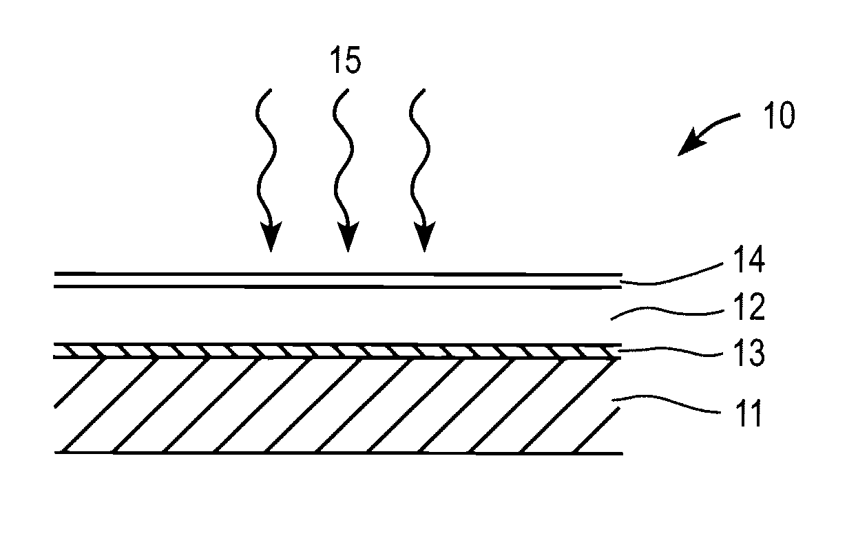
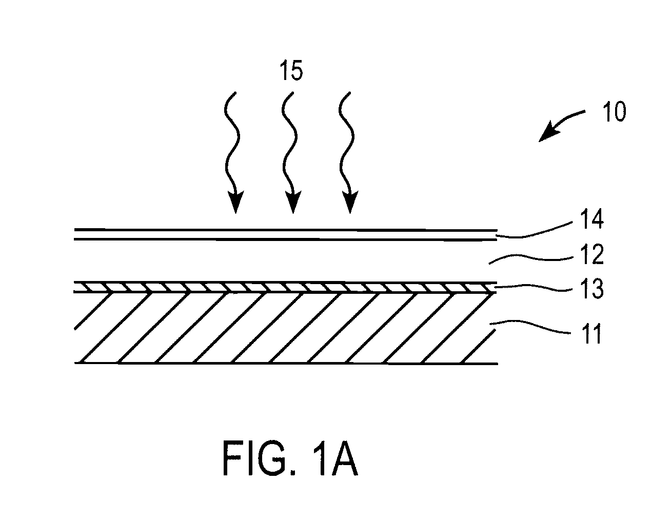
[0029] A Cu(In,Ga)Se2 compound layer with a Cu / (In+Ga) ratio of 0.95 and Ga / (Ga+In) ratio of 0.3 may be grown using the present invention by first depositing a Cu / In / Ga precursor stack on a substrate and then reacting the stack with selenium, i.e. by selenizing the stack. It is straight forward to calculate that if the thickness of the Cu sub-layer in the stack is 200 nm, an In sub-layer thickness of 325 nm and a Ga sub-layer thickness of 104 nm would be needed to provide the target composition defined above. In processing such a precursor stack, the following steps may be carried out: i) a nominally 200 nm thick Cu sub-layer may be first deposited on at least one portion of a substrate at a first deposition station using optimized conditions and in-situ thickness control means, ii) deposited Cu sub-layer thickness on the portion of the substrate may be determined at a metrology or measurement station, iii) if the thickness measured is within an acceptable range (such as within + / −5...
example 2
[0031] Let us now take, as an example, an electroplating technique used to manufacture Cu / In / Ga precursor stacks on a large number of substrates, such as hundreds or thousands of substrates which may each be 1 ft×1 ft or 1 ft×4 ft in size. Starting with a fresh Cu plating solution or electrolyte, it may be possible to deposit accurately the 200 nm thick Cu layer on the substrates early in the process by applying a pre-determined current density for a pre-determined time. As more and more substrates are electroplated, however, the electrolyte may start to age and the plating efficiency of Cu may drop from its initial value, which may be in the range of 70-100% depending on the chemistry used. Therefore, although the early substrates receive nominally 200 nm thick Cu, the Cu thickness on later substrates may start to decrease. If this reduction of Cu thickness goes un-detected and if the In and Ga thicknesses are accurate, the Cu / (In+Ga) molar ratio in the precursor stack would be low...
example 3
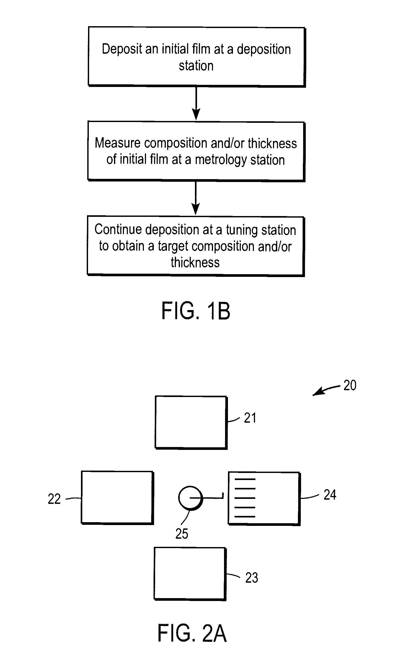
[0032] In a two-stage process employing an electrodeposited Cu—Ga / In precursor stack, the process may be carried out as follows: A Cu—Ga alloy may be first deposited on a substrate in the form of an initial film at a deposition station. The substrate may then be moved to a metrology station to determine the molar Cu and Ga content in this initial film. If more Cu is needed to reach the target composition, the substrate may be forwarded to a tuning station that deposits more Cu on the initial film. If more Ga is needed to reach the target composition, the substrate may be forwarded to a tuning station that deposits more Ga on the initial film. Once the Cu and Ga contents are brought to a targeted range an In sub-layer may be deposited to form the precursor stack. Indium sub-layer deposition may also be divided into at least two steps. In the first step an In initial film may be deposited over the Cu and Ga containing sub-layer. At a metrology station In content may be measured. Then ...
PUM
 Abstract
Description
Claims
Application Information


