

CMOS process with Si gates for nFETs and SiGe gates for pFETs
- Summary
- Abstract
- Description
- Claims
- Application Information
AI Technical Summary
Benefits of technology
Problems solved by technology
Method used
Image

Examples
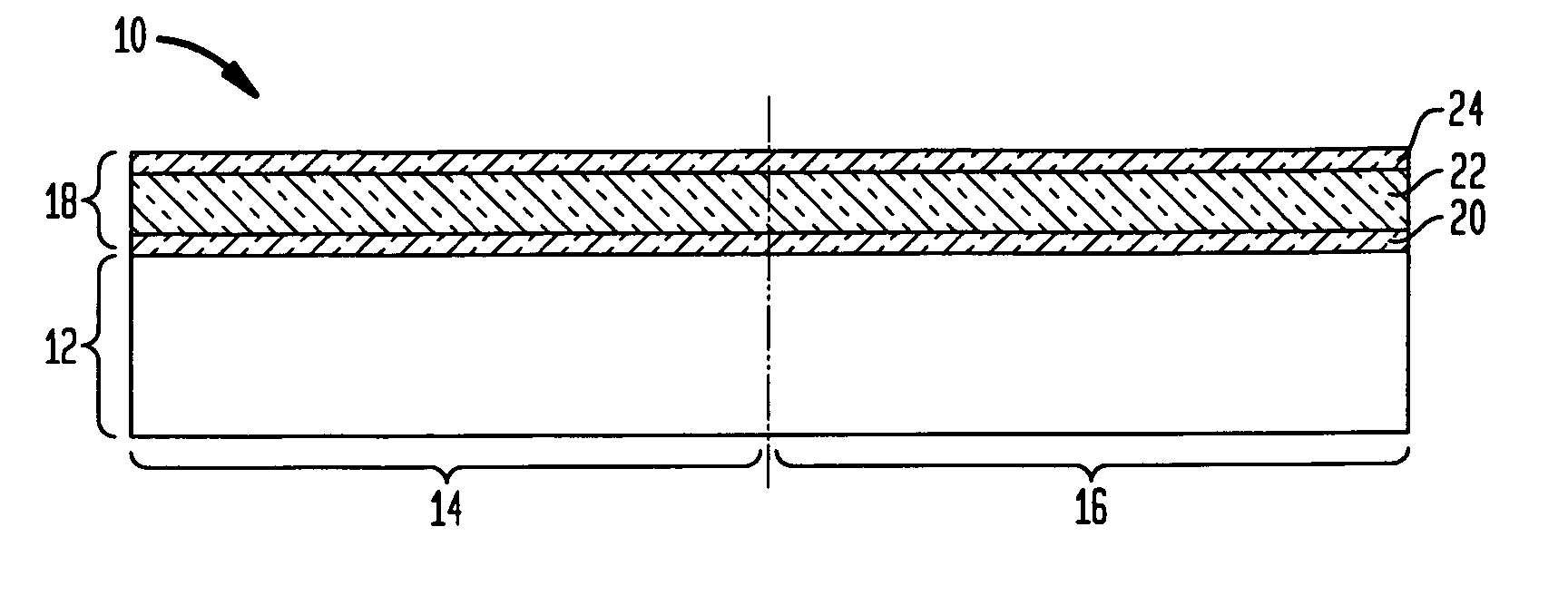
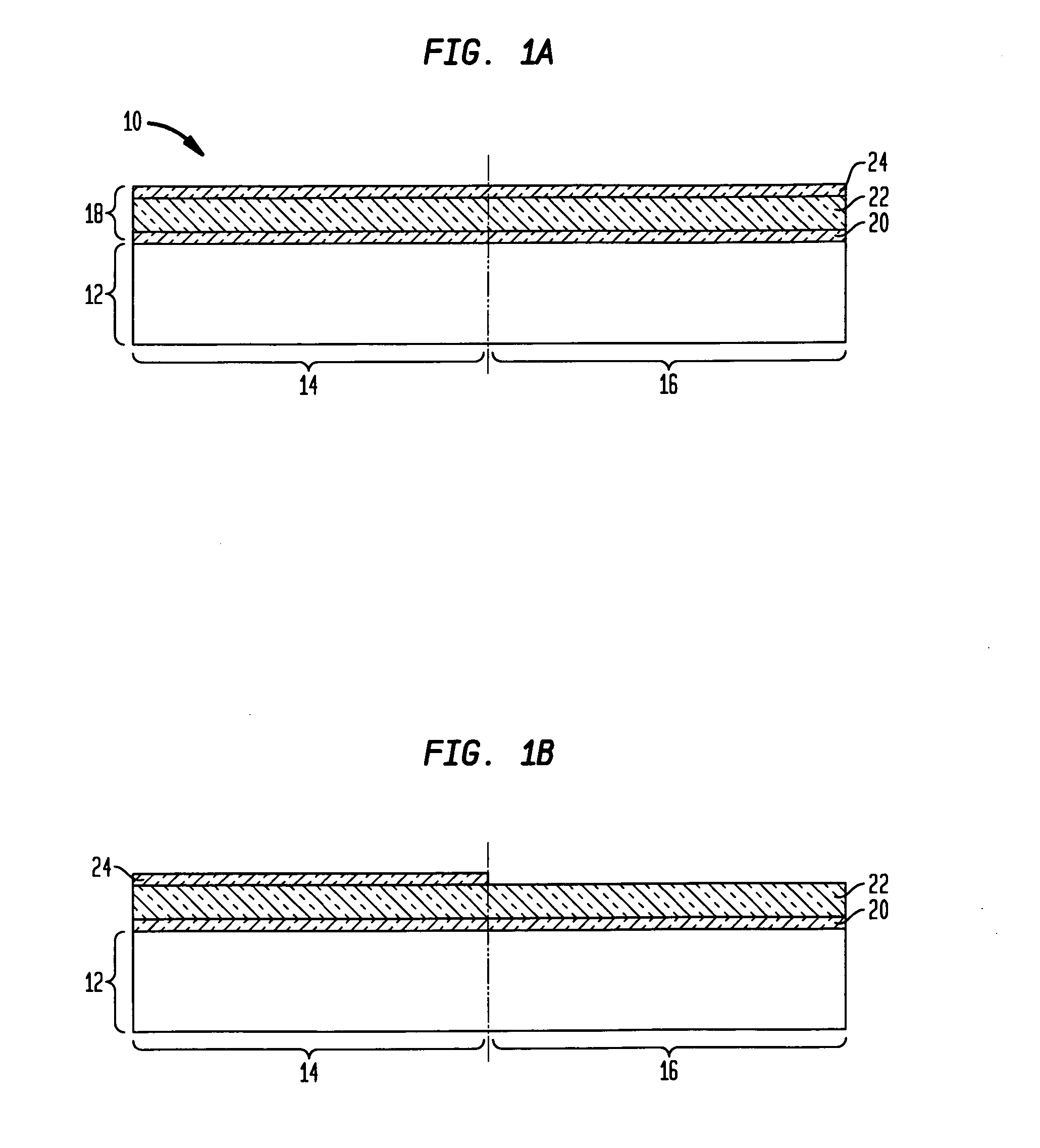
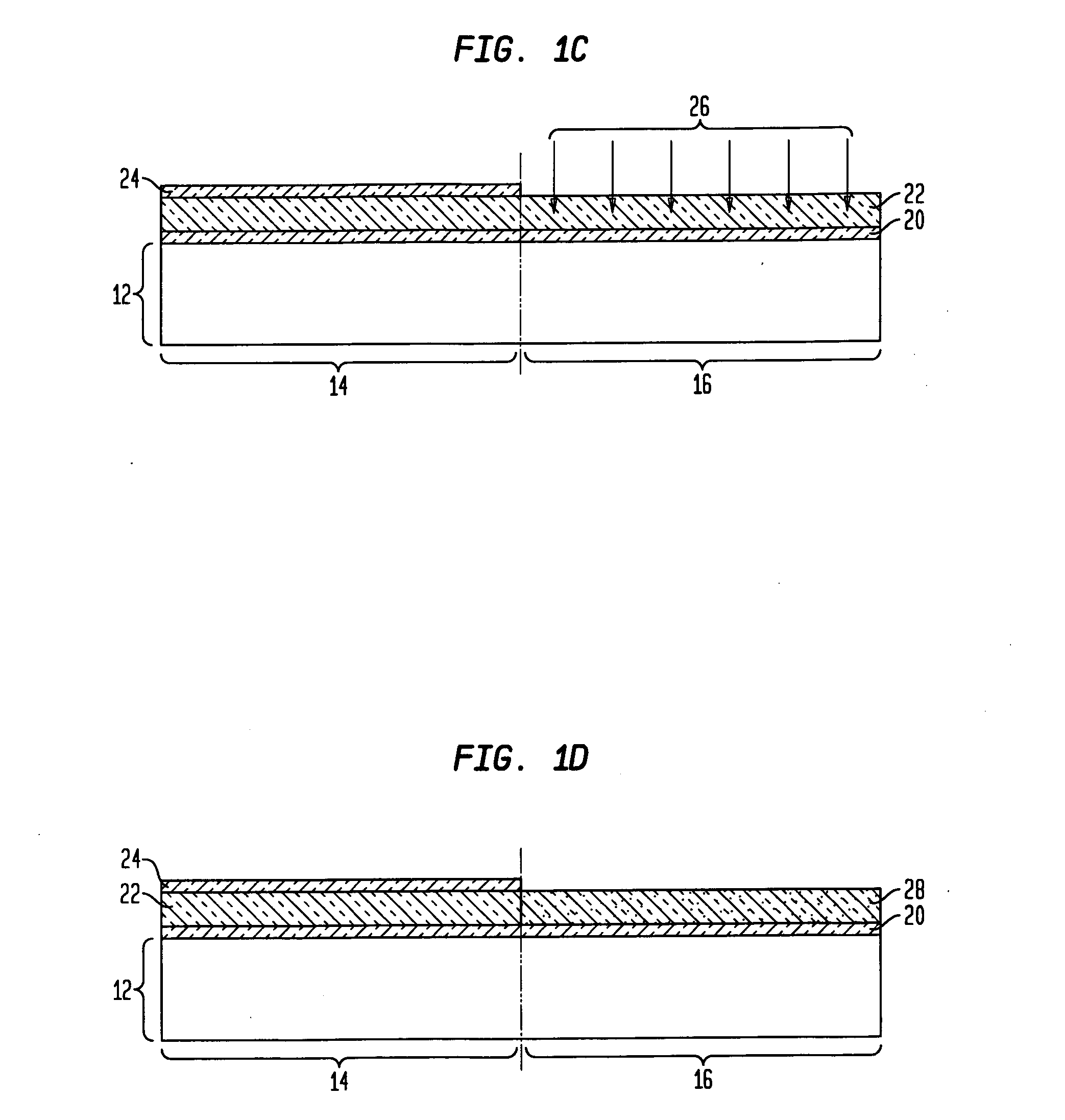
first embodiment
[0030] At this point of the present invention, Ge atoms 26 are introduced into the exposed portion of the Si film such as is shown in FIG. 1C. The Ge atoms 26 are introduced by first providing a Ge-containing source gas into a reactor chamber including the structure shown in FIG. 1B and then heating the Ge-containing source gas at a temperature that is sufficient to cause decomposition of the Ge-containing source gas into at least Ge atoms. The Ge-containing source gas used in the present invention includes a GeaXb compound wherein each X is the same or different and is H (Hydrogen), Cl (Chlorine) or metallorganic compounds, a is 1 or 2, and b is 2, 4 or 6. Preferably, the Ge-containing source gas is GeH4.
[0031] After providing the Ge-containing source gas into the reactor chamber, the Ge-containing source gas is heated to a temperature of about 200° C. or greater, with a temperature from about 350° to about 800° C. being even more typical. The temperature used in the present invent...
third embodiment
[0053] Note that an oxide layer (not shown) is typically formed atop the SiGe layer 52 during the thermal oxidation process of the present invention. The surface oxide layer is typically, but not always, removed from the structure after the heating step using a conventional wet etch process wherein a chemical etchant such as HF that has a high selectivity for removing oxide as compared to SiGe is employed. During this etching step, and in instances wherein the remaining hard mask 24 atop the nFET region 14 is an oxide, the remaining oxide hard mask 24 can be removed.
[0054] The surface oxide layer formed after the thermal oxidation step of the present invention has a variable thickness which may range from about 10 to about 1000 nm, with a thickness of from about 20 to about 500 nm being more highly preferred.
[0055] The heating temperature used to ‘thermally mix’ layers 50 and 22 which is a function of Ge content in the Ge-containing layer 50, may be from about 200° C. to about 1300...
PUM
 Abstract
Description
Claims
Application Information