Semiconductor device having fuse element and method of cutting fuse element

a technology of a fuse element and a device body, which is applied in the direction of semiconductor devices, semiconductor/solid-state device details, electrical devices, etc., can solve the problems of heavy damage on the member, and achieve the effect of effectively absorbing the energy of the laser beam, and small damage on the part located above or below the fuse elemen

Inactive Publication Date: 2007-10-11
ELPIDA MEMORY INC
View PDF3 Cites 1 Cited by
  • Summary
  • Abstract
  • Description
  • Claims
  • Application Information

AI Technical Summary

Benefits of technology

[0019]According to the present invention, a fuse element is arranged such that it passes through at least first and second insulating films, resulting in a vertically long configuration of the fuse element. Thus, it is possible to effectively absorb the energy of a laser beam by the fuse element, so that when the fuse element is cut by using an optical system of which the depth of focus is smaller than the height of the fuse element, the damage imposed on a part located above or below the fuse element is very small.
[0020]According to the present invention, the fuse element is arranged such that it passes through the second insulating film of which the absorptivity of light is large, so that in an area where the fuse element passes through the second insulating film, it is possible to effectively absorb the energy of the laser beam. As are result, it becomes possible to cut the fuse element by using a laser beam of which power is as low as possible, so that it becomes possible to reduce damage imposed on a part above or below the fuse element as much as possible.
[0021]When an optical system of which the depth of focus is small is used, a margin of focal positions in the up and down directions decreases. However, according to the present invention, it becomes possible to sufficiently secure the margin of the focal positions in the up and down directions. In particular, recently, a warpage of a semiconductor wafer chronically occurs as the semiconductor wafer grows in size. Due to this tendency, a deviation of the focal positions in the up and down directions occurs very easily. However, according to the present invention, the deviation of the focal positions, which is caused due to the warpage of the semiconductor wafer, can also be solved. This can be explained according to the reasons as follows.
[0022]That is, when a laser beam is irradiated such that the second insulating film of which the absorptivity of light is large remains within the depth of focus or in the vicinity thereof, even if the focal point slightly deviates upwardly or downwardly, most of energy of the laser beam is absorbed by the second insulating film, so that an area where the fuse element penetrates the second insulating film will always be destructed first. Destruction stress concentrates onto the area destructed first, so that areas not intended to be irradiated are not to draw the stress. Due to these phenomena, in the present invention, the deviation of the focal positions in the up and down directions is substantially compensated. Accordingly, the margin of the focal positions in the up and down directions increases.
[0023]In such optical system, the objective lens having a large numerical aperture is used, so that the energy density imposed on the passivation film is very small, compared to the conventional case. As a result, it is possible to cut the fuse element without destructing the passivation film.
[0024]The damage imposed above or below the fuse element is very small, so that it is also possible to arrange a wiring or a transistor above or below the fuse element. Since the objective lens having a large numerical aperture is used, the beam spot at a position deviated from the focal point is made very large, compared to the conventional case. Thus, it is possible to greatly narrow the distance between the adjacent fuse elements.

Problems solved by technology

However, there are various problems including imposing of heavy damage on members, for example, the passivation film, existing immediately above or below the fuse element.

Method used


Image

  • Semiconductor device having fuse element and method of cutting fuse element
  • Semiconductor device having fuse element and method of cutting fuse element
  • Semiconductor device having fuse element and method of cutting fuse element

Examples


first embodiment

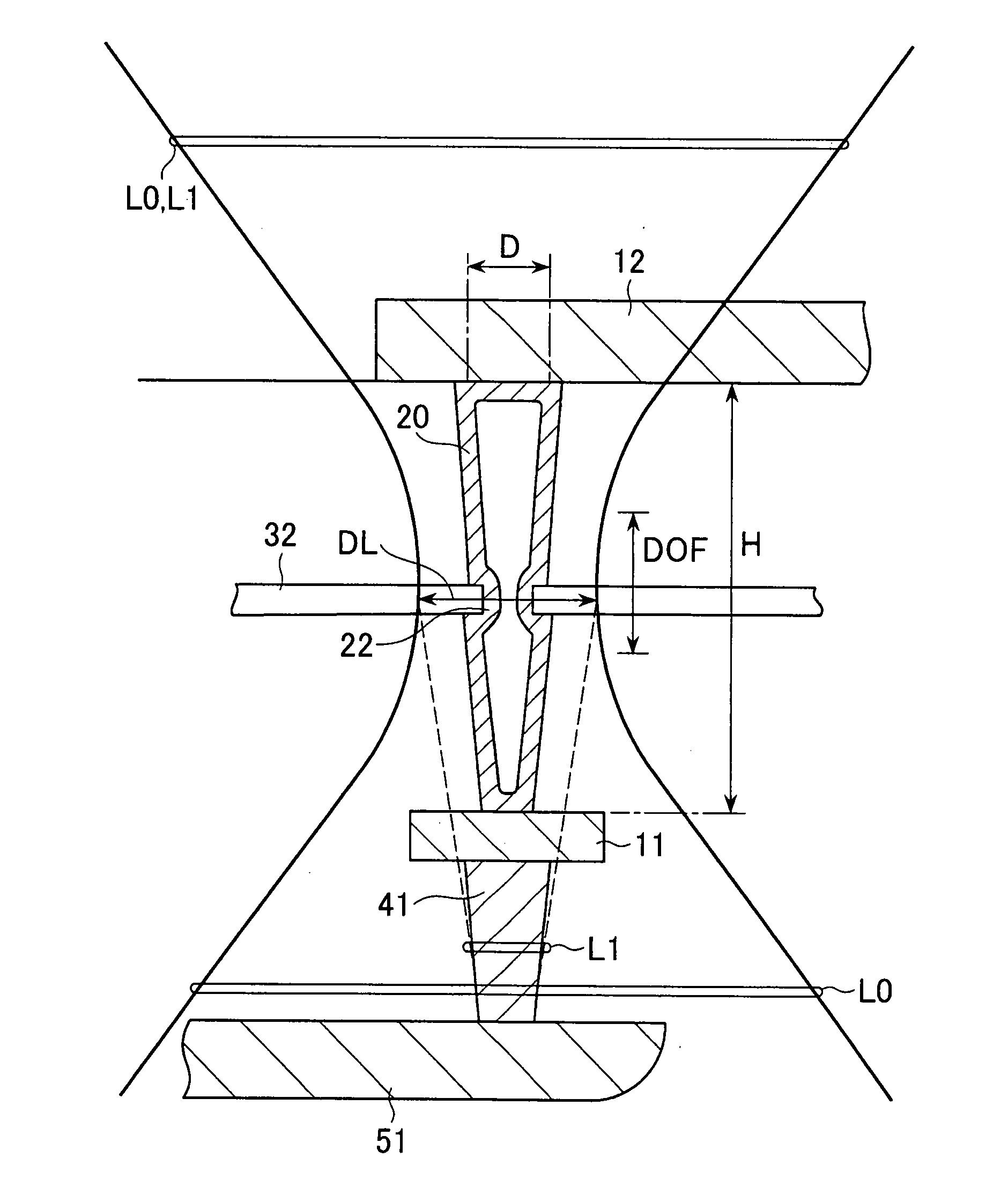
[0045]FIG. 1 is a schematic cross section of the structure of a fuse element included in a semiconductor device according to a preferred first embodiment of the present invention.

[0046]As shown in FIG. 1, the semiconductor device according to the first embodiment includes a lower electrode 11, an upper electrode 12, and a fuse element 20 that connects the lower electrode 11 and the upper electrode 12. The lower electrode 11 and the upper electrode 12 are electrodes formed in different wiring layers. Between the both electrodes, there exit three layers of insulating films 31 to 33 stacked in this order viewed from the side of the lower electrode 11. Accordingly, the fuse element 20 that connects these components have a height equal to the total thickness of the insulating films 31 to 33 that separate the lower electrode 11 and the lower electrode 12.

[0047]The fuse element 20 has a tubular shape with a hollow portion 20a therein, as shown in FIG. 1. The hollow portion 20a contains gas...

second embodiment

[0108]the present invention is explained next.

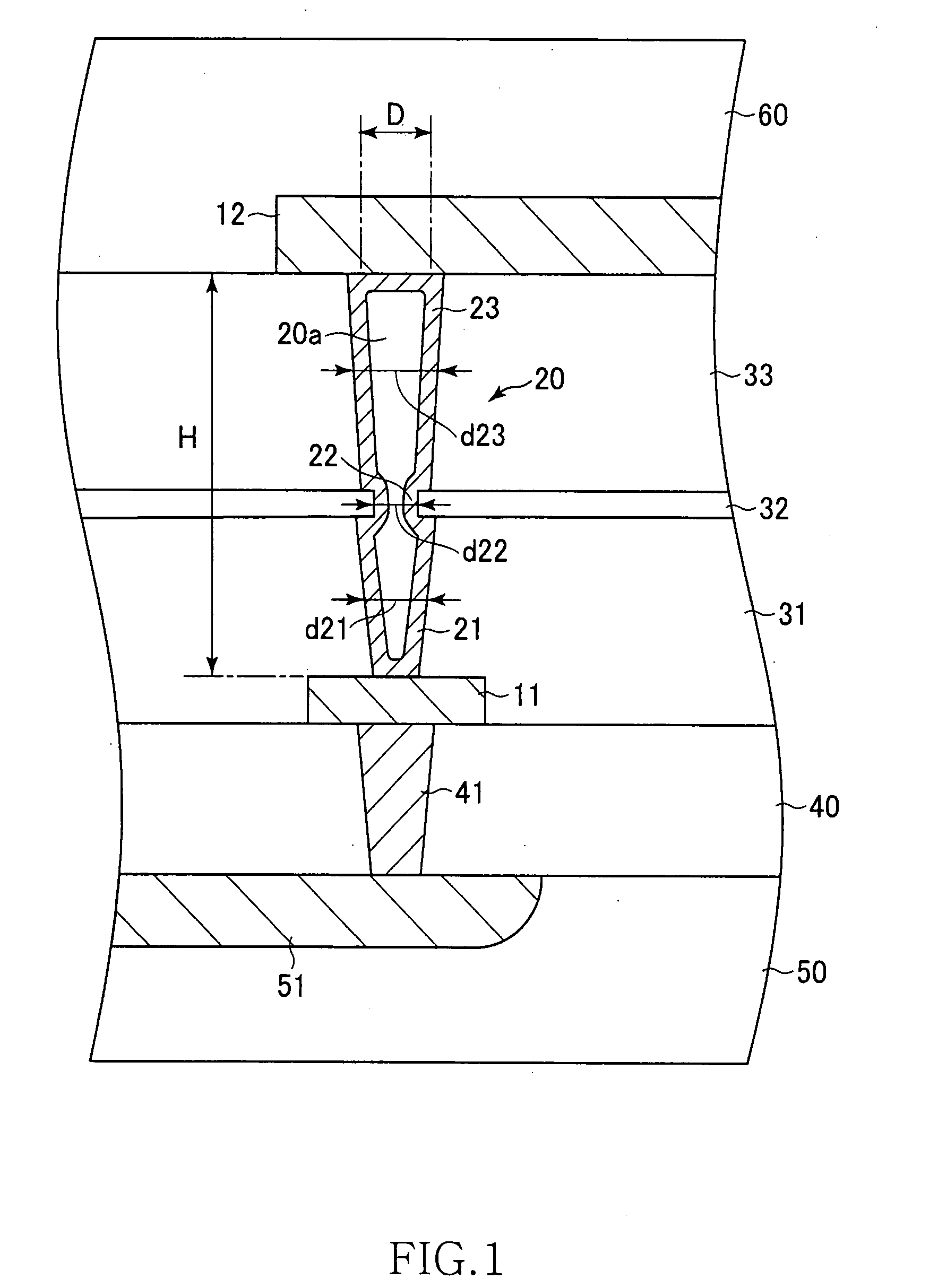
[0109]FIG. 17 is a schematic cross section of the structure of a fuse element included in a semiconductor device according to a preferred second embodiment of the present invention.

[0110]As shown in FIG. 17, the semiconductor device according to the present embodiment is different from the semiconductor device according to the first embodiment in that the second embodiment includes, between the lower electrode 11 and the upper electrode 12, four layers of insulating films 31 to 34 stacked in this order viewed from the side of the lower electrode 11, and the fuse element 20 includes a fourth tubular portion 24 that passes through the insulating film 34. Since other features of this embodiment are basically the same as that of the semiconductor device according to the first embodiment, like parts are designated by like reference numerals, and redundant explanations will be omitted.

[0111]The added insulating film 34 is an insulating film lo...


PUM


Abstract

A semiconductor device includes a lower electrode, an upper electrode, and a fuse element that connects the lower electrode and the upper electrode. Between the lower electrode and the upper electrode, insulating films stacked in this order exist. Out of the insulating films, the insulating film located in the middle has absorptivity of light larger than those of the other insulating films. Thus, in the present invention, a fuse element that is vertically long and penetrates an insulating film of which the absorptivity of light is large in the central portion is used, so that it is possible to effectively absorb energy of a laser beam. Further, it is possible to cut the fuse element using an optical system having a small depth of focus, so that it is possible to cut the fuse element without destructing a passivation layer.

Description

TECHNICAL FIELD[0001]The present invention relates to a semiconductor device, and more particularly, to a semiconductor device having a fuse element that can be cut by irradiation with a laser beam. The present invention also relates to a method of cutting a fuse element, and more particularly, to a method of cutting a fuse element by irradiation with a laser beam.BACKGROUND OF THE INVENTION[0002]The storage density of a semiconductor memory device represented by a DRAM (Dynamic Random Access Memory) is increasing year by year due to advancement in a microfabrication technique. Along with the progress in downsizing, the number of defective memory cells included per one chip is also increasing. Generally, such defective memory cell is replaced by a redundant memory cell, thereby relieving a defective address.[0003]Generally, the defective address is stored in a program circuit including a plurality of fuse elements. When the defective address is accessed, the program circuit detects ...

Claims


Application Information

Patent Timeline
Patent Type & Authority Applications(United States)
IPC IPC(8): H01L29/00
CPCH01L23/5258H01L2924/0002H01L2924/00
Inventor OGAWA, SUMIO
Owner ELPIDA MEMORY INC
Why Eureka
Try Eureka