

High Performance Light-Emitting Devices
a light-emitting device, high-performance technology, applied in the direction of thermoelectric device junction materials, semiconductor devices, electrical apparatus, etc., can solve the problems of short life, poor stability, and the performance of an oled degrades quickly, and achieves high efficiency, high efficiency, and maximize external extraction efficiency
- Summary
- Abstract
- Description
- Claims
- Application Information
AI Technical Summary
Benefits of technology
Problems solved by technology
Method used
Image

Examples
embodiment
Third Type of Embodiment
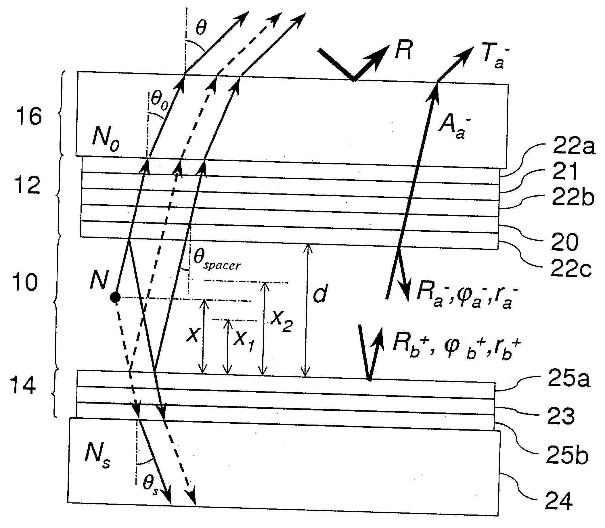
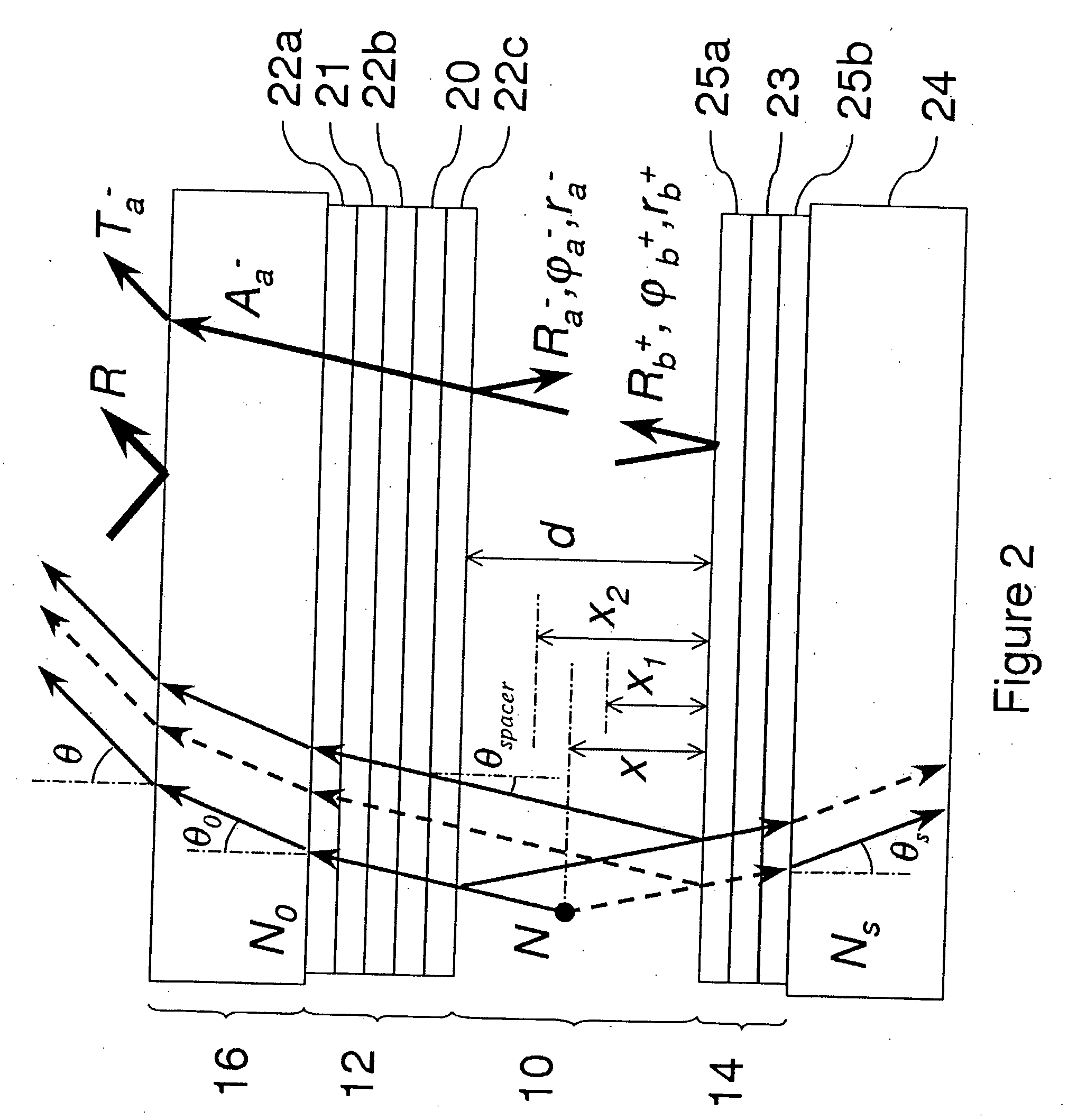
[0090] The intent of the third type of embodiments in accordance with the present invention is to obtain OLED devices with good efficiency, good contrast (low external reflectance) and good angular field by introducing in the top multilayer stack additional metal and dielectric layers before- or metal layers after the ITO layer. The layer structure and thicknesses of these added layers are optimized to minimize the external reflectance of the whole OLED structure and at the same time to retain a good efficiency and angular field based on the teachings of the present invention. It should be appreciated that the external reflectance of the structure, that is the reflectance of the whole OLED structure to light impinging on the structure from outside needs to be minimized in order to maximize the contrast of the device, while as noted above the internal reflectance needs to be maximized in order to enhance the microcavity effect.
[0091] In embodiment C1 in accor...
PUM
 Abstract
Description
Claims
Application Information