Light Emitting Element and Method of Manufacturing the Same

a technology of light-emitting elements and semiconductor devices, which is applied in the direction of semiconductor lasers, polycrystalline material growth, crystal growth process, etc., can solve the problems of insufficient crystallinity, failure to obtain epitaxial films having low threading dislocation density, and mismatch between the layers, so as to achieve low cost and highluminance characteristics

Active Publication Date: 2007-10-25
SOPHIA UNIVERSITY
View PDF9 Cites 117 Cited by
  • Summary
  • Abstract
  • Description
  • Claims
  • Application Information

AI Technical Summary

Problems solved by technology

However, since crystal lattice of the (0001) surface of the sapphire substrate and that of the (0001) surface of the nitride-base compound semiconductor differ in the lattice constants, there is lattice mismatch between them.
Thus, growth of the nitride-base compound semiconductor layer onto the sapphire substrate results in an insufficient crystallinity as a continuous thin film, and fails in obtaining an epitaxial film having a low threading dislocation density.
Presence of a high density of such threading dislocation results in degradation in light emitting characteristics, when the nitride-base compound semiconductor is used as a material for high-luminance light emitting diodes and semiconductor lasers.

Method used


Image

  • Light Emitting Element and Method of Manufacturing the Same
  • Light Emitting Element and Method of Manufacturing the Same
  • Light Emitting Element and Method of Manufacturing the Same

Examples


Embodiment Construction

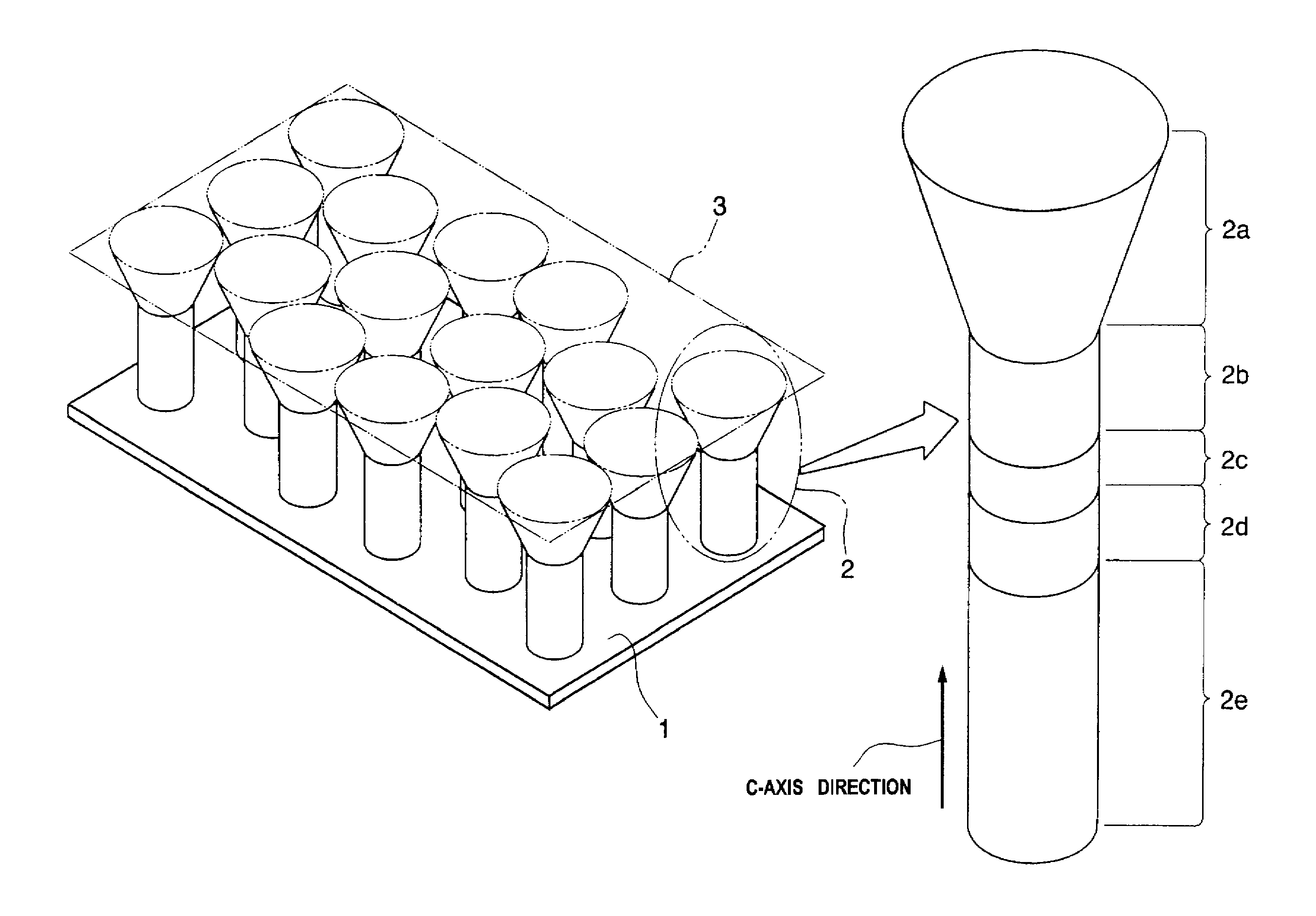
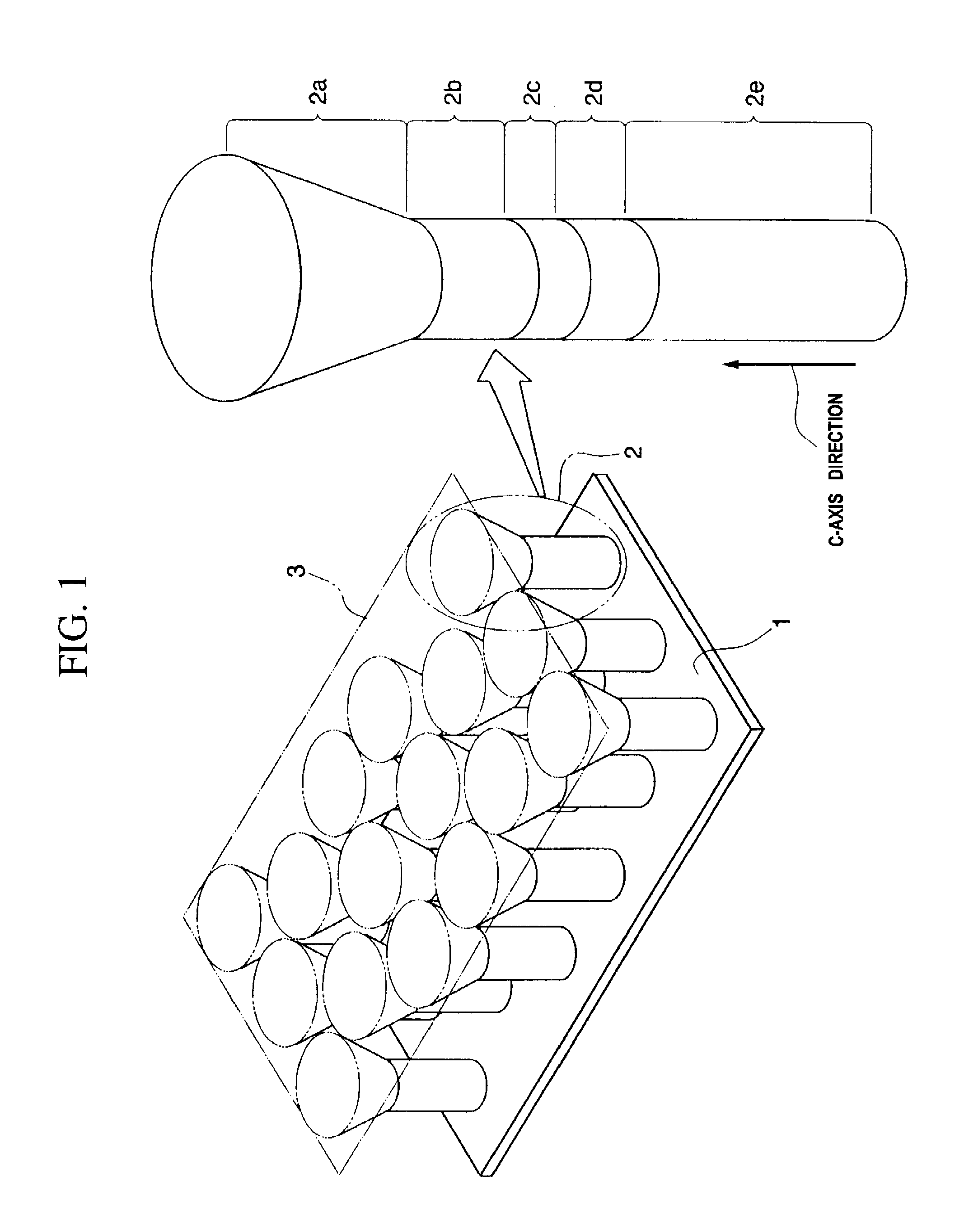
[0052] Paragraphs below will explain a structure of the light emitting element (light emitting diode, for example) according to one embodiment of the present invention referring to the attached drawings. FIG. 1 is a block diagram showing a structure of the light emitting element according to this embodiment.

[0053] As seen in this drawing, a light emitting element L has columnar crystals 2 formed on the top surface of a substrate 1, wherein the upper portion of the columnar crystals 2 are electrically connected to an electrode layer 3.

[0054] Each of the columnar crystals 2 has, as a device structure, as shown by the enlarged view on the right hand side in FIG. 1, a reverse pyramid (reverse cone or reverse polygonal pyramid) portion 2a (p-type cladding layer), an i-type blocking layer 2b, a light emitting layer 2c, an i-type blocking layer 2d, and an n-type cladding layer 2e.

[0055] The columnar crystal 2 has such device structure as described in the above, containing the light emit...


PUM

PropertyMeasurementUnit
temperatureaaaaaaaaaa

Abstract

A method of manufacturing a semiconductor element by forming, on a substrate, columnar crystals of a nitride-base or an oxide-base compound semiconductor, and by using the columnar crystals, wherein on the surface of the substrate, the columnar crystals are grown while ensuring anisotropy in the direction of c-axis, by controlling ratio of supply of Group-III atoms and nitrogen, or Group-II atoms and oxygen atoms, and temperature of crystal growth, so as to suppress crystal growth in the lateral direction on the surface of the substrate.

Description

TECHNICAL FIELD [0001] The present invention relates to a semiconductor element of semiconductor devices, such as diode, light emitting diode and semiconductor laser, which is obtained by allowing a nitride-base or oxide-base compound semiconductor layer to grow according to a predetermined density in a form of uniform columnar crystals, and by using thus-grown columnar crystals, and a method of manufacturing the same. [0002] This application is to claim a right of priority over Japanese Patent Application No. 2004-253267 filed on 31 Aug., 2004, the content of which is incorporated hereinto by reference. BACKGROUND ART [0003] Nitride-base compound semiconductors are known to show direct transition over the entire compositional region thereof (for example, AlN, GaN, InN and mixed crystals thereof), have wide band gaps, and are known as materials for blue or violet light emitting diode, in other words, materials for short-wavelength light emitting elements. [0004] The nitride-base com...

Claims


Application Information

Patent Timeline
Patent Type & Authority Applications(United States)
IPC IPC(8): H01S5/183H01L33/00H01L33/08H01L33/20
CPCB82Y20/00H01L21/02603C30B29/16C30B29/403C30B29/605H01L33/007H01L33/0079H01L33/08H01L33/20H01S5/021H01S5/041H01S5/183H01S5/3202H01S5/3412H01S5/34333C30B23/002H01L21/0237H01L21/02381H01L21/0242H01L21/02458H01L21/02472H01L21/02483H01L21/02505H01L21/0254H01L21/02554H01L21/02565C30B25/02H01L33/0093H01L33/18H01S5/320225H01L21/0262H01S2304/04
Inventor KIKUCHI, AKIHIKOKISHINO, KATSUMI
Owner SOPHIA UNIVERSITY
Why Eureka
Try Eureka