Method for the production of thin substrates

a technology of thin substrates and substrates, applied in the field of thin substrates, can solve the problems of high production and market growth, deep shortage of silicon feedstock, and high price of commercially available silicon solar modules, and achieve the effects of high efficiency, high efficiency, and high efficiency

Inactive Publication Date: 2007-10-25
KATHOLIEKE UNIV LEUVEN
View PDF4 Cites 141 Cited by
  • Summary
  • Abstract
  • Description
  • Claims
  • Application Information

AI Technical Summary

Benefits of technology

[0047]Providing a mother substrate that is not significantly bent or elastically deformed when inducing the stress can favor the conservation of the integrity of the mother substrate after the release of the thin substrate and the use of the mother substrate several times for successive thin substrate releases. The mother substrate can for example be an ingot, and the so-called thin substrate can be a typical substrate for semiconductor processing, such as a substrate having a thickness not higher than 750 μm, e.g. a 600 or 750 μm thick substrate.
[0048]The thin substrate can have a thickness below 750, 600, 500, 400, 300, 200, 150, 100, 90, 80, 70, 60, 50, 40, 30, 20, or 10 μm, depending on the thickness of the mother substrate. The thin substrate can have a thickness larger than 10 nm, 100 nm, 1 μm, 5 μm. Thin substrates below 300, 200, 150, 100, 90, 80, 70, 60, 50, 40, 30, 20, or 10 μm may particularly be interesting to be obtained by this method since the standard method for obtaining such thin substrates is wire sawing, which induces a kerf loss in the range of 200 μm lost for one wafer sawn. In addition, for photovoltaic applications such as solar cell applications, it may be interesting to obtain thin substrates thinner than what is currently available. The price of a commercia

Problems solved by technology

But a major issue is currently threatening the impressive 40% annual growth of both market and production: the world of photovoltaics is currently undergoing a deep silicon feedstock shortage [Photon International].
In addition, the price of a commercially available silicon solar module is driven by the cost of the semiconductor material which represents by itself almost half of the production cost of the finished module.
At the moment, silicon wafering (e.g. for solar cells) is still performed by wire saw techniques, which bring an important kerf loss of around 200 μm per wafer.
The relative loss i

Method used


Image

  • Method for the production of thin substrates
  • Method for the production of thin substrates
  • Method for the production of thin substrates

Examples


Embodiment Construction

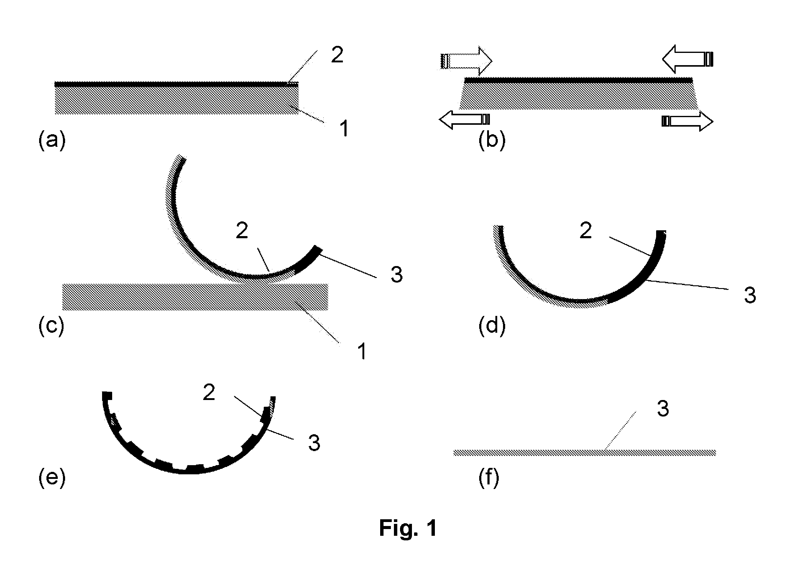
[0094]The present invention will be described with respect to particular embodiments and with reference to certain drawings but the invention is not limited thereto but only by the claims. The drawings described are only schematic and are non-limiting. In the drawings, the size of some of the elements may be exaggerated and not drawn on scale for illustrative purposes.

[0095]Furthermore, the terms first, second, third and the like in the description and in the claims, are used for distinguishing between similar elements and not necessarily for describing a sequential or chronological order. It is to be understood that the terms so used are interchangeable under appropriate circumstances and that the embodiments of the invention described herein are capable of operation in other sequences than described or illustrated herein.

[0096]Moreover, the terms top, bottom, over, under and the like in the description and the claims are used for descriptive purposes and not necessarily for descri...


PUM


Abstract

A method is provided for producing a thin substrate with a thickness below 750 microns, comprising providing a mother substrate, the mother substrate having a first main surface and a toughness; inducing a stress with predetermined stress profile in at least a portion of the mother substrate, said portion comprising the thin substrate, the induced stress being locally larger than the toughness of the mother substrate at a first depth under the main surface; such that the thin substrate is released from the mother substrate, wherein the toughness of the mother substrate at the first depth is not lowered prior to inducing the stress. The method can be used in the production of, for example, solar cells.

Description

CROSS-REFERENCE TO RELATED APPLICATIONS[0001]This application claims the benefit under 35 U.S.C. § 119(e) of U.S. provisional application Ser. No. 60 / 793,098, filed Apr. 19, 2006, and claims the benefit under 35 U.S.C. § 119(a)-(d) of European application No. 06011050, filed May 30, 2006, the disclosures of which are hereby expressly incorporated by reference in their entirety and are hereby expressly made a portion of this application.FIELD OF THE INVENTION[0002]The present invention relates to the field of thin substrates. More particularly the present invention relates to a method for producing a thin substrate with a thickness below 750 micron. The method according to embodiments of the invention can be used in the production of, for example, solar cells.BACKGROUND OF THE INVENTION[0003]Nowadays' production of solar cells mainly relies on silicon. Crystalline silicon solar cells (including multi-crystalline and single-crystal) account for 90% of solar cell production [http: / / www...

Claims


Application Information

Patent Timeline
IPC IPC(8): H01L21/30H01L21/46
CPCH01L21/30H01L21/304H01L31/0392Y02E10/547H01L31/182Y02E10/546H01L31/1804Y02P70/50
Inventor DROSS, FREDERICVAN KERSCHAVER, EMMANUELBEAUCARNE, GUY
Owner KATHOLIEKE UNIV LEUVEN
Why Eureka
Try Eureka