Check patentability & draft patents in minutes with Patsnap Eureka AI!

Method to manufacture a coreless packaging substrate

a manufacturing method and packaging technology, applied in the direction of printed circuit manufacturing, printed circuit aspects, non-metallic protective coating applications, etc., can solve the problems of serious compromise in the manufacture of multi-layer substrates, the thickness of the final multi-layer substrate cannot be reduced, and the use of higher frequencies or operations at higher speeds is restricted. , to achieve the effect of reducing the thickness of the substrate, raising the wiring density

Active Publication Date: 2007-10-25
PHOENIX PRECISION TECH CORP
View PDF13 Cites 13 Cited by
  • Summary
  • Abstract
  • Description
  • Claims
  • Application Information

AI Technical Summary

Benefits of technology

[0012]In light of the shortcomings of the prior arts described above, the main objective of the present invention is to provide a method of manufacturing a packaging substrate, which can raise the wiring density and reduce the thickness of substrate, to thereby meet the developmental trend of miniaturization.
[0013]Another objective of the present invention is to simplify process steps, raise yield, shorten manufacture time, and reduce manufacture cost.
[0021]Thereby the coreless packaging substrates prepared by the present invention have higher layout integration, simpler manufacturing procedures, and reduced general product thickness, and the goal of miniaturization is achieved.
[0023]Besides, the method of the present invention can further comprise a step (H) after forming the solder bumps and the solder layers in step (G): attaching at least a metal supporting frame on the surface of the first solder mask, so as to increase overall rigidity of the substrate.
[0024]In addition, the method of the present invention can further comprise a step (F1) before forming the solder bumps in the second openings and forming the solder layers in the third openings: forming a third metal layer as a post in at least one of the second openings in the first solder mask and the third openings in the second solder mask along with the fourth openings in the first dielectric layer, to thereby reduce the quantity of solder material needed for the solder bumps as well as the solder layers.

Problems solved by technology

Though high-number leads can be obtained compared with lead frames, usage on higher frequencies or operations at higher speed are restricted due to limited performance of the package structure attributed to lacks of both shorter paths of leads due to the core thickness and higher wiring density due to the land width of through holes.
As a result, the thickness of the final multi-layer substrate cannot be reduced, which is unfavorable to the developmental trend of a miniaturized semiconductor package structure.
If the thickness of the core substrate is reduced to as thin as 60 μm or less, the manufacture of the multi-layer substrate will be seriously compromised, and the yield from the manufacture of substrate will decrease significantly.
In addition, there are extra steps in the manufacture of the core substrate, such as the hole-plugging and the scrubbing, which elevate the manufacture cost.
In comparison, the process of plating through holes makes it more difficult to form a structure with finer circuits.
Moreover, in the process of multi-layer substrate described above, it is required to manufacture a core substrate prior to forming dielectric layers and circuit layers, which consequently complicates the process steps and increases the manufacture time, and raises the manufacture cost as well.
As a result, it is urgent for the industry to avoid the drawbacks of the previous technique, such as the increased thickness of substrate, low wiring density, low yield, complicated process steps, elevated manufacture time and cost.

Method used


Image

  • Method to manufacture a coreless packaging substrate
  • Method to manufacture a coreless packaging substrate
  • Method to manufacture a coreless packaging substrate

Examples


Embodiment Construction

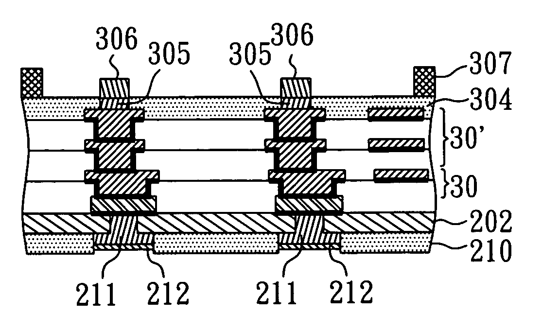
[0029]FIGS. 2A to 2P are the cross-sections of a preferred embodiment of the present invention. First, as shown in FIG. 2A, a carrier board 201 is provided; then as shown in FIG. 2B, a first dielectric layer 202 made of ABF (Ajinomoto Build-up Film) is formed on the carrier board 201, wherein a seed layer 225 is formed on the first dielectric layer 202 to facilitate subsequent electroplating process. Referring to FIG. 2C, a first resistive layer 226 is formed on the surface of the seed layer 225, and a plurality of first openings 226a are formed in the first resistive layer by photolithography to expose the seed layer 225. Subsequently, as shown in FIG. 2D, a first metal layer 227 is formed by electroplating in each of the first openings 226a. In this example, the seed layer 225 and the first metal layers 227 are copper layers, and the first metal layer 227 serves an electrical connection.

[0030]Then referring to FIG. 2E, the first resistive layer 226 is removed, and the seed layer 2...


PUM

PropertyMeasurementUnit
thicknessaaaaaaaaaa
diameteraaaaaaaaaa
diameteraaaaaaaaaa

Abstract

A method for manufacturing a coreless packaging substrate is disclosed. The method can produce a coreless packaging substrate which comprises: at least a built-up structure having a first solder mask and a second solder mask, wherein a plurality of openings are formed in the first and second solder mask to expose the conductive pads of the built-up structure; and a plurality of solder bumps as well as solder layers formed on the conductive pads. Therefore, the invention can produce the coreless packaging substrate with high density of circuit layout, less manufacturing steps, and small size.

Description

BACKGROUND OF THE INVENTION[0001]1. Field of the Invention[0002]The present invention relates to a method to manufacture a coreless packaging substrate, particularly a method to manufacture a coreless packaging substrate that is applicable to non-through hole structures, to thereby increases density of circuit layout, and streamlines manufacture process.[0003]2. Description of Related Art[0004]With the development of the electronic industry, the research is gradually turning to high integration and miniaturization to meet the demands of multi-function, high speed, and high frequency for electronic products. Accordingly in semiconductor packaging, the circuit boards providing circuit connections among active and passive components are evolving from single layer boards to multi-layer boards in order to expand available areas of circuit layout on circuit boards within limited spaces by interlayer connection techniques, so as to accommodate higher wiring density for integrated circuits....

Claims


Application Information

Patent Timeline
Patent Type & Authority Applications(United States)
IPC IPC(8): H01L21/4763
CPCH01L21/4857H01L21/6835H01L2924/0002H01L23/49822H05K1/113H05K3/0035H05K3/007H05K3/108H05K3/243H05K3/28H05K3/4007H05K3/4682H05K2201/09436H05K2201/09563H05K2201/096H05K2203/0152H05K2203/0376H01L2924/00
Inventor CHEN, BO-WEIWANG, HSIEN-SHOUHSU, SHIH-PING
Owner PHOENIX PRECISION TECH CORP
Features
  • R&D
  • Intellectual Property
  • Life Sciences
  • Materials
  • Tech Scout
  • Unparalleled Data Quality
  • Higher Quality Content
  • 60% Fewer Hallucinations
Learn More