Compound and organic light-emitting element

a light-emitting element and organic compound technology, applied in the direction of discharge tube luminescnet screen, other domestic articles, natural mineral layered products, etc., can solve the problems of affecting the material having entirely satisfactory light-emission luminance and durability, and the performance of the present device has not been satisfactory, etc., to achieve high efficiency and highly luminant light emission, easy manufacturing, and high durability

Inactive Publication Date: 2007-10-25
CANON KK
View PDF7 Cites 22 Cited by
  • Summary
  • Abstract
  • Description
  • Claims
  • Application Information

AI Technical Summary

Benefits of technology

[0013]The present invention provides a novel compound used for organic EL elements, that has a molecular structure represented by the following general formula (1) and an organic EL element using the same, that has highly efficient and highly luminant...

Problems solved by technology

In addition, there have been many problems in durability, such as changes in performance after long term use and degradation thereof caused, for example, by an oxygen-containing gas and/or moisture.
However, for this application, prese...

Method used


Image

  • Compound and organic light-emitting element
  • Compound and organic light-emitting element
  • Compound and organic light-emitting element

Examples


example 1

Synthesis of Exemplified Compound No. D-2

[0053]

[0054]The compound 1-1 (manufactured by Aldrich Chemical Company, Inc.) in an amount of 344 mg (2 mmole), 566 mg (2 mmole) of the compound 1-2, 40.1 g of Pd (PPh3), 10 ml of toluene, 5 ml of ethanol, and 10 ml of an aqueous sodium carbonate solution at a concentration of 2 M were charged in an eggplant flask having a volume of 100 ml and were then stirred for 8 hours at 40° C. under a nitrogen stream. After the reaction was completed, crystals were obtained by filtration, followed by washing using water, ethanol, and toluene. The crystals thus obtained were dried by evacuation at 120° C., so that 340 mg (at a yield of 60%) of the compound 1-3 was obtained.

[0055]The compound 1-3 in an amount of 800 mg (2.44 mmole), 830 mg (2.68 mmole) of the compound 1-4, 40.05 g of Pd (PPh3), 10 ml of toluene, 5 ml of ethanol, and 10 ml of an aqueous sodium carbonate solution at a concentration of 2 M were charged in an eggplant flask having a volume of...

example 2

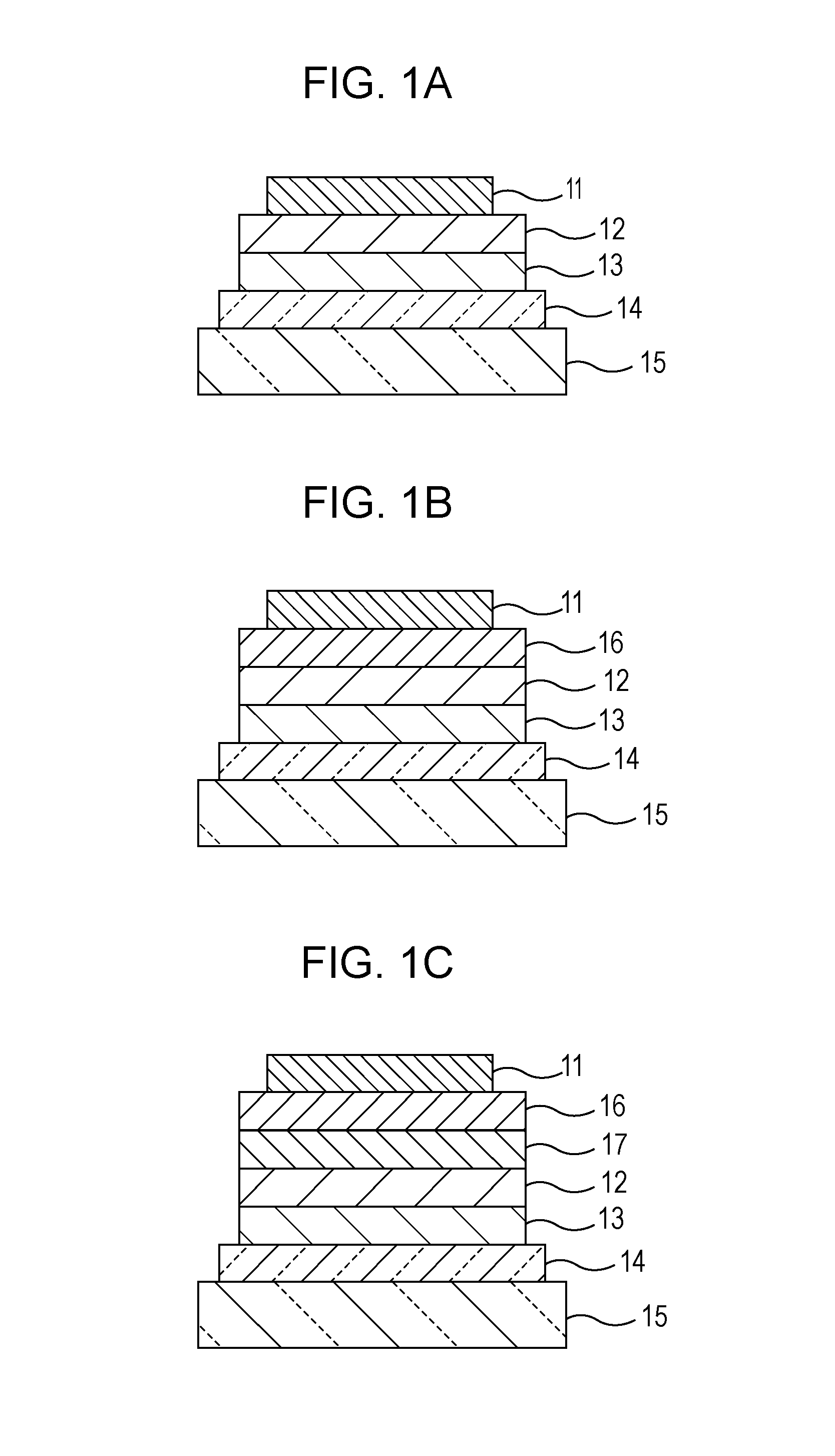
[0061]In this example, an element having the three organic layers shown in FIG. 1B was used. An ITO film having a thickness of 100 nm was patterned on a glass substrate. On this ITO substrate, the following organic layers and the electrode layer were sequentially formed in a vacuum chamber at a pressure of 10−5 Pa by vacuum evaporation using resistance heating so as to obtain a facing electrode area of 3 mm2.[0062]Hole transport layer (40 nm): Compound 2[0063]Light-emitting layer (50 nm): Compound 3 and the exemplified compound D-2 (weight ratio of 5%)[0064]Electron transport layer (25 nm): Compound 4[0065]Metal electrode layer 1 (0.5 nm): LiF[0066]Metal electrode layer 2 (100 nm): Al

[0067]As for properties of the EL element, current-voltage properties were measured by an ammeter 4140B manufactured by Hewlett-Packard Co., and the light emission luminance was measured by BM7 manufactured by Topcon Corp. It was confirmed that the element of this example is a blue light emission elemen...

example 3

[0068]An element was formed in a manner similar to that in Example 2 except that the exemplified compound No. D-1 was used instead of the exemplified compound No. D-2 of Example 2. The element of this example was a blue light emission element, and the luminance and the light emission efficiencies were 6.4 cd / A and 4.9 lm / W (at 400 cd / m2), respectively. In addition, the current density at an application voltage of 5 V was 39 mA / cm2.


PUM

PropertyMeasurementUnit
Nanoscale particle sizeaaaaaaaaaa

Abstract

A high-performance organic light-emitting element and a novel organic compound realizing the above element are provided. A fluoranthene compound having a specific structure and an organic light-emitting element using the same are provided.

Description

BACKGROUND OF THE INVENTION[0001]1. Field of the Invention[0002]The present invention relates to light-emitting elements using an organic compound, and more particularly, relates to a compound having a molecular structure represented by general formula (1) shown below and an organic electroluminescent (EL) element having stable high efficiency by using the above compound for a light-emitting layer or a charge transport layer.[0003]2. Description of the Related Art[0004]In the past, light emission was typically performed by applying a voltage to an anthracene-deposited film (Thin Solid Films, 94 (1982) 171).[0005]In addition, as particularly described in Macromol. Symp. 125, 1 to 48 (1997), typically, an organic EL element has a structure in which top and bottom electrodes are formed on a transparent substrate and organic material layers, including a light-emitting layer, are provided between the electrodes.[0006]In addition, when various types of fluorescent organic compounds are us...

Claims


Application Information

Patent Timeline
IPC IPC(8): H01L51/54C09K11/06C07C13/66
CPCC07C13/66C07C43/21C07C2103/40H05B33/14C09K2211/1011H01L51/0054H01L51/5012C09K11/06Y10S428/917C07C2603/40H10K85/622H10K50/11
Inventor IWAWAKI, HIRONOBUNEGISHI, CHIKAOKADA, SHINJIROTAKIGUCHI, TAKAOSENOO, AKIHIROHASHIMOTO, MASASHI
Owner CANON KK
Why Eureka
Try Eureka