

Electro-optical device, electronic apparatus, and method of manufacturing electro-optical device
- Summary
- Abstract
- Description
- Claims
- Application Information
AI Technical Summary
Benefits of technology
Problems solved by technology
Method used
Image

Examples
first exemplary embodiment
Overall Configuration of an Embodiment of a Liquid Crystal Device
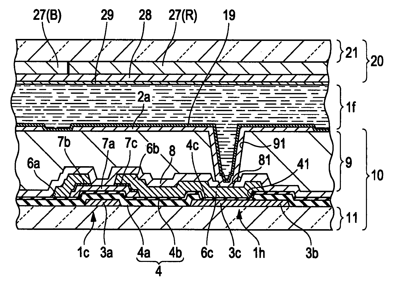
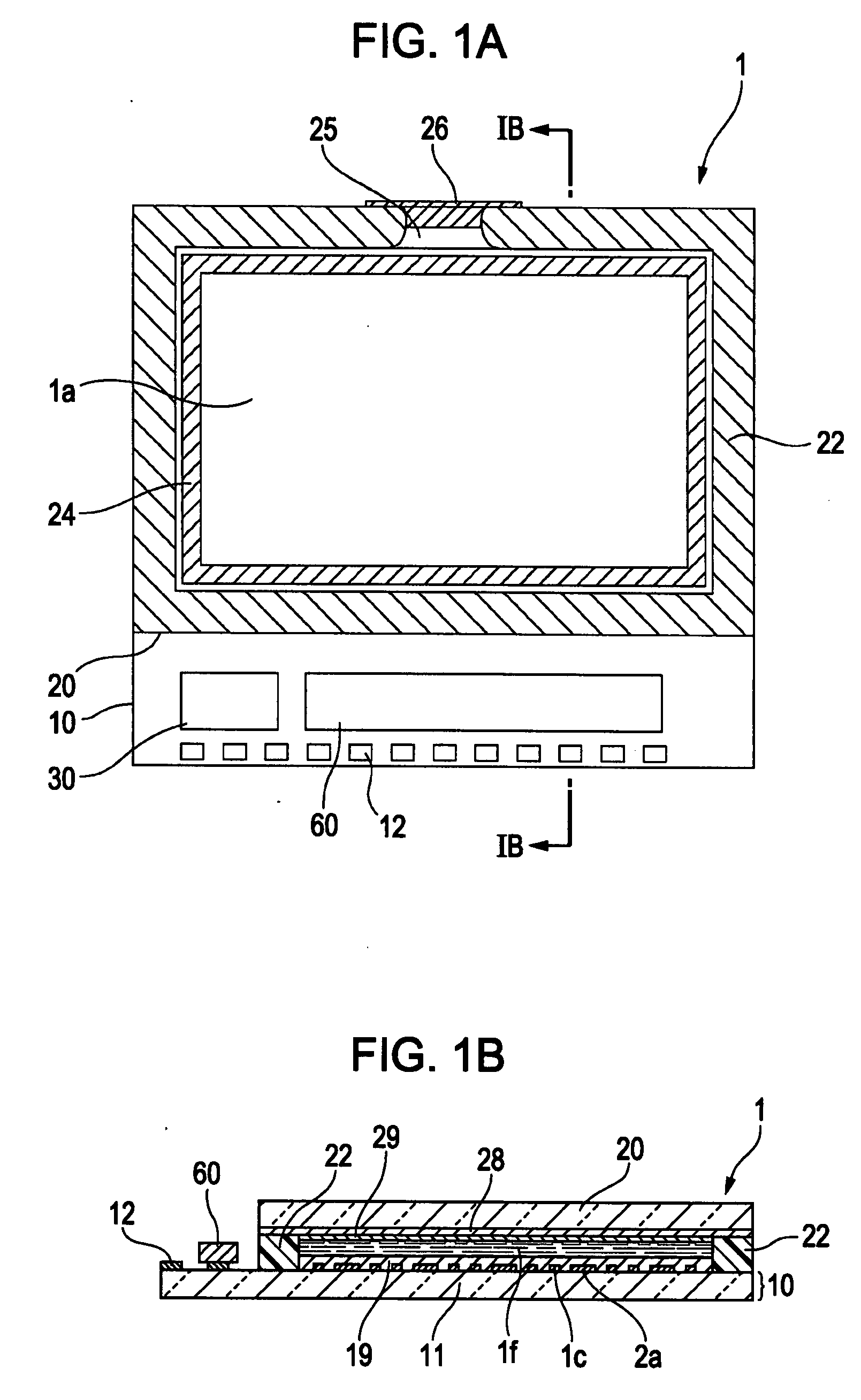
[0043]FIGS. 1A and 1B are a plan view of a liquid crystal device (electro-optical device) together with the constituent elements formed thereon as viewed from a counter substrate, and a cross-sectional view taken along the line IB-IB, respectively. FIGS. 1A and 1B show a liquid crystal device 1 of this embodiment which may be a TN (Twisted Nematic) mode, an ECB (Electrically Controlled Birefringence) mode, or a VAN (Vertical Aligned Nematic) mode transmissive active matrix liquid crystal device. In the liquid crystal device 1, an element substrate 10 and a counter substrate 20 are bonded to each other using a sealant 22 with liquid crystal 1f interposed therebetween. In the element substrate 10, a data line driving IC 60 and a scanning line driving IC 30 are mounted by a COG (Chip On Glass) method in an end region outside the sealant 22, and mounting terminals 12 are formed along the sides of the substrate. The sealant...
second exemplary embodiment
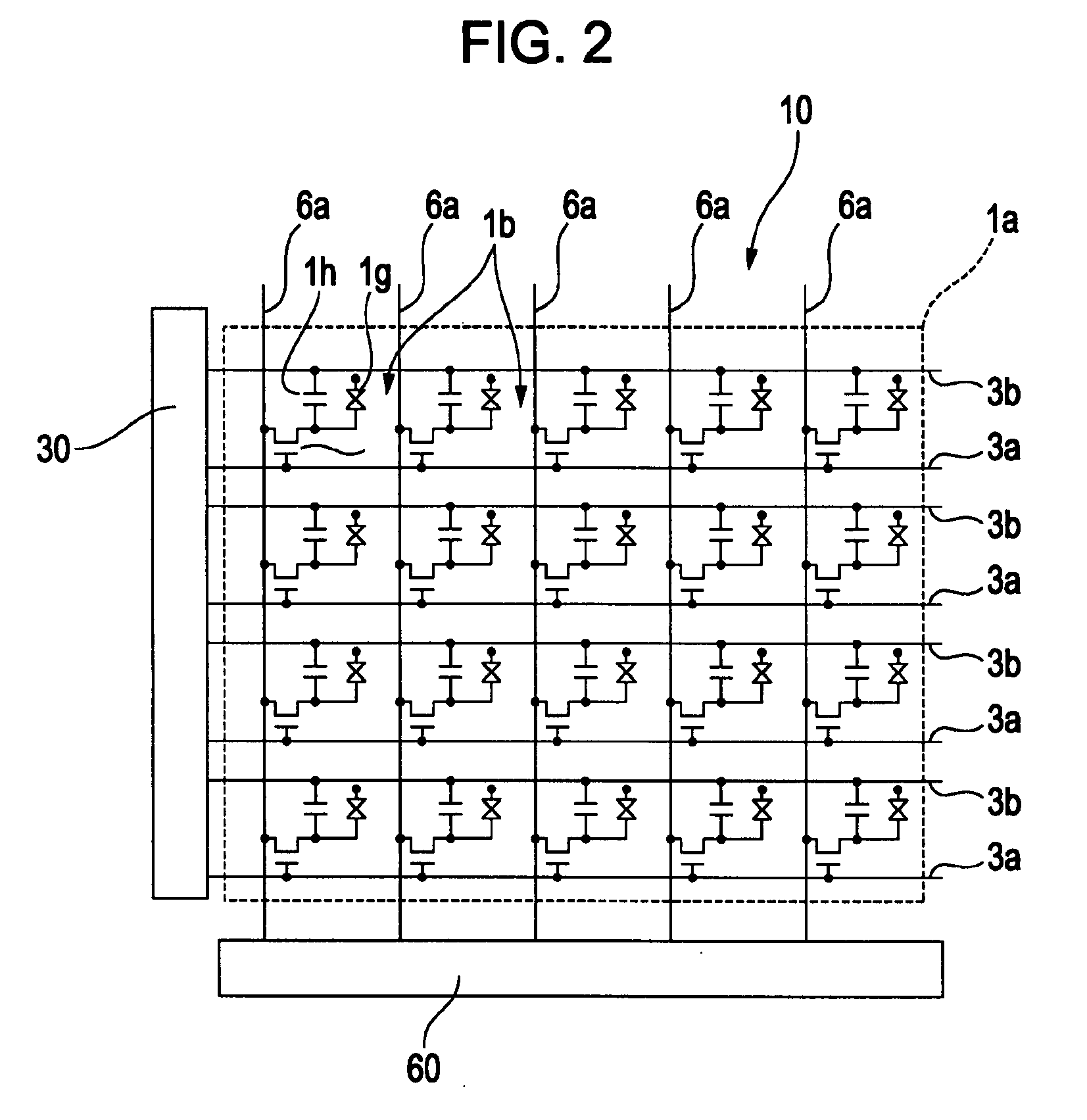
[0075]FIGS. 6A and 6B are a plan view of one pixel in a liquid crystal device according to a second exemplary embodiment, and a cross-sectional view of the liquid crystal device taken along the line VIB-VIB, respectively. FIGS. 7A to 7G are process cross-sectional views showing steps until the source and drain electrodes are formed, in a manufacturing process of the element substrate 10 that is used in the liquid crystal device 1 of this embodiment. In FIG. 6A, the pixel electrode is indicated by a bold and long dotted line, the gate line and the thin film formed along with the gate line are indicated by a thin solid line, the source line and the thin film formed along with the source line are indicated by a thin one-dot-chain line, and the semiconductor layer is indicated by a thin and short dotted line. Further, a portion corresponding to dielectric layer constituting the storage capacitor is indicated by a thin two-dot-chain line, and the contact hole is indicated by a thin solid...
third exemplary embodiment
[0085]FIGS. 8A and 8B are a plan view of one pixel in a liquid crystal device according to a third exemplary embodiment, and a cross-sectional view of the liquid crystal device taken along the line VIIIB-VIIIB, respectively. FIGS. 9A to 9G are process cross-sectional views showing steps until the source and the drain electrodes are formed, in a manufacturing process of the element substrate 10 that is used in the liquid crystal device 1 of this embodiment. In FIG. 8A, the pixel electrode is indicated by a bold and long dotted line, the gate line and the thin film formed along with the gate line are indicated by a thin solid line, the source line and the thin film formed along with the source line are indicated by a thin one-dot-chain line, and the semiconductor layer is indicated by a thin and short dotted line. Further, the portion corresponding to the dielectric layer constituting the storage capacitor is indicated by a thin two-dot-chain line, and the contact hole is indicated by...
PUM
 Abstract
Description
Claims
Application Information