Semiconductor device and method for manufacturing the semiconductor device

Inactive Publication Date: 2007-11-01
SEMICON ENERGY LAB CO LTD
View PDF36 Cites 247 Cited by
  • Summary
  • Abstract
  • Description
  • Claims
  • Application Information

AI Technical Summary

Benefits of technology

[0029]With the use of the present invention, separation into a plurality of element regions can be performed without division of the semiconductor layer into island shapes, and a plurality of semiconductor elements can be manufactured. Accordingly, a step is not generated in an edge portion of the semiconductor layer, and a gate insulating layer is formed over the plane semiconductor layer. Therefore, coverage of the semiconductor layer with the gate insulating layer is impro

Problems solved by technology

However, in the above method for moderating a step, defects such as a short between a semiconductor layer due to a contact and a gate electrode and a leakage current cannot be sufficiently prevented depending on a thickness of the sem

Method used


Image

  • Semiconductor device and method for manufacturing the semiconductor device
  • Semiconductor device and method for manufacturing the semiconductor device
  • Semiconductor device and method for manufacturing the semiconductor device

Examples


embodiment mode 1

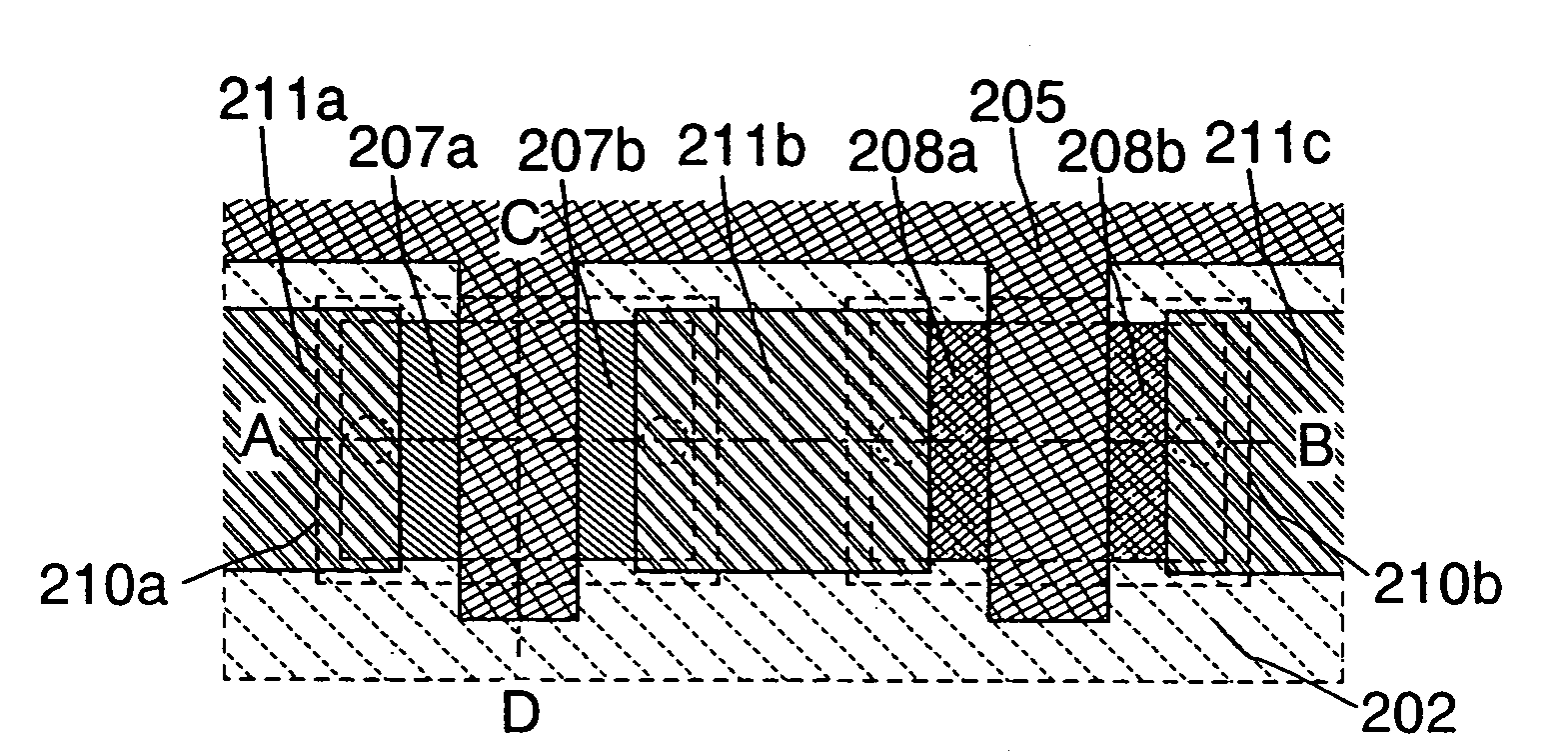
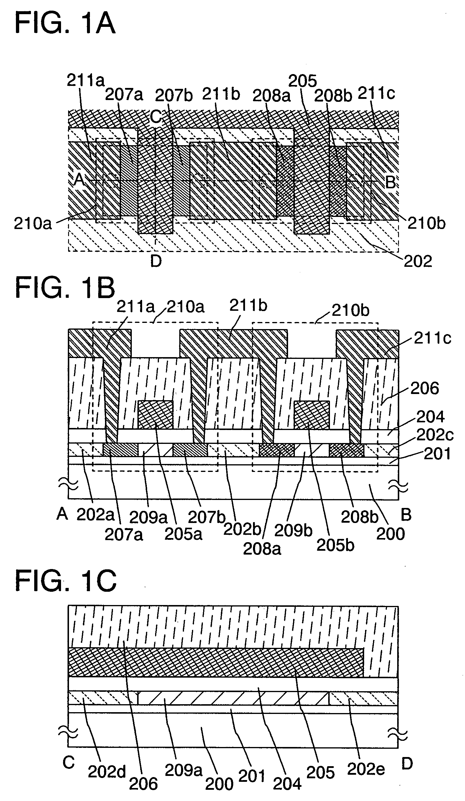
[0057]In this embodiment mode, as an example of a semiconductor device intended to prevent defectes such as a short between a gate electrode layer and a semiconductor layer and a leakage current due to insufficient coverage of the semiconductor layer with a gate insualting layer and to give higher reliablility, a CMOS (Complementary Metal Oxide Semiconductor) will be explained with reference to drawings.

[0058]FIGS. 1A to 1C show an example of a semiconductor device having a CMOS structure of this embodiment mode. FIG. 1A is a top view, FIG. 1B is a cross-sectional view taken along a line A-B in FIG. 1A, and FIG. 1C is a cross-sectional view taken along a line C-D in FIG. 1A.

[0059]Over a substrate 200 over which an insulating layer 201 serving as a base film for a semiconductor layer is formed, a CMOS structure made of a transistor 210a and a transistor 210b that are an n-channel thin film transistor and a p-channel film transistor, respectively, and an insulating layer 206 are forme...

embodiment mode 2

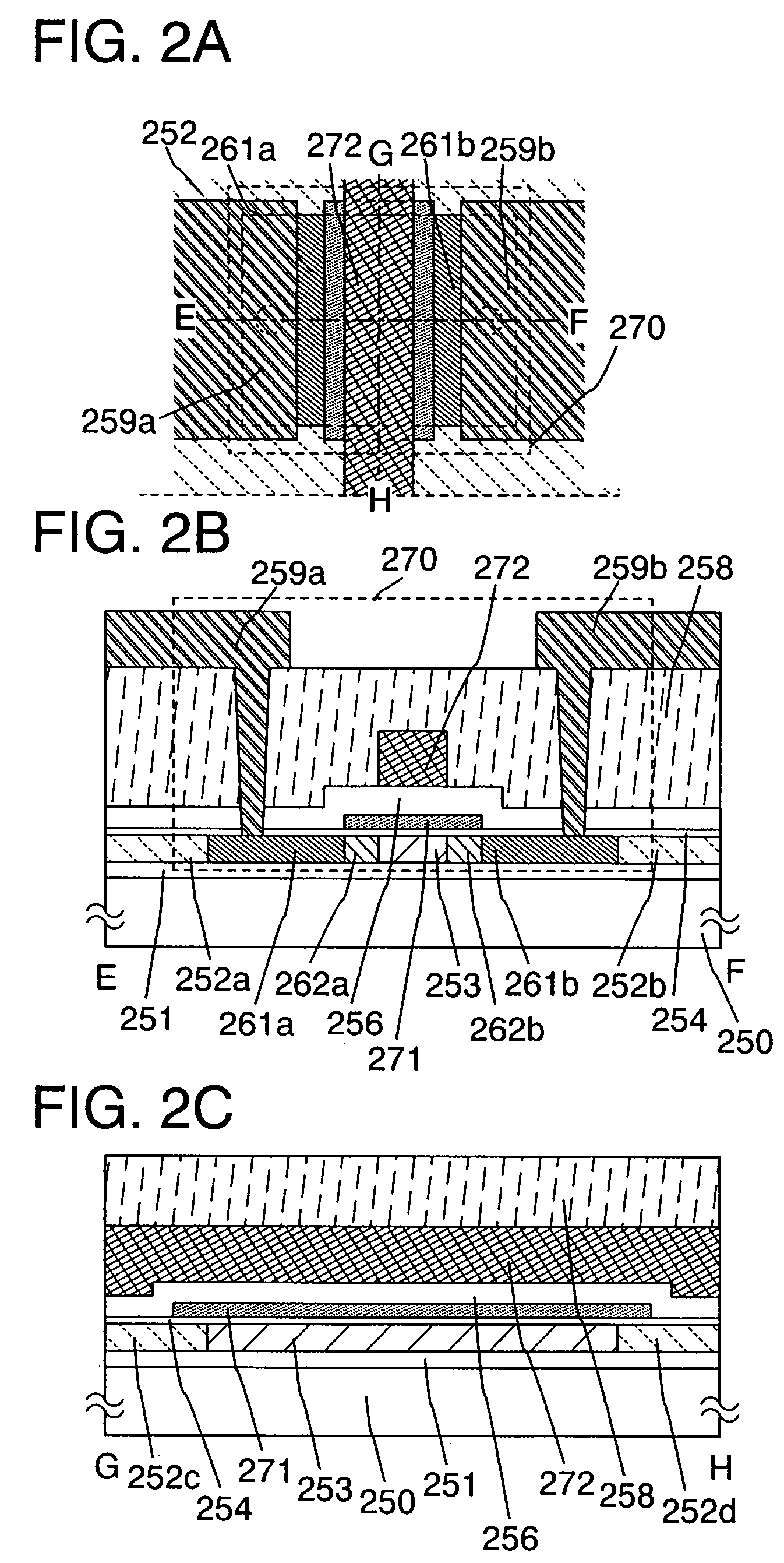
[0084]In this embodiment mode, as a semiconductor device intended to prevent defects such as a short between an electrode layer and a semiconductor layer and a leakage current due to insufficient coverage of the semiconductor layer with an insulating layer and to give higher reliability, an example of a nonvolatile semiconductor storage device will be explained with reference to drawings.

[0085]A nonvolatile storage element has a similar structure to a MOSFET (Metal Oxide Semiconductor Filed Effect Transistor) and a feature that a region capable of accumulating charges for a long period is provided over a channel formation region. This charge accumulating region is formed over an insulating layer and insulated from circumference; thus, it is also referred to as a floating gate electrode layer. In addition, the floating gate electrode layer is referred to as a charge accumulating layer because it has a function for accumulating charges. In the present specification, this charge accumu...

embodiment mode 3

[0142]In this embodiment mode, an example of a semiconductor device will be explained with reference to drawings, which has a memory element (also referred to as a storage element) intended to prevent defects such as a short between a gate electrode layer and a semiconductor layer and a leakage current due to insufficient coverage of the semiconductor layer with an insulating layer in a semiconductor element and to give higher reliability. FIG. 15 shows a top view of a semiconductor device of this embodiment mode, FIG. 16A shows a cross-sectional view taken along a line I-L in FIG. 15, and FIG. 16B shows a cross-sectional view taken along a line K-L in FIG. 15.

[0143]FIG. 15 shows a NOR-type equivalent circuit in which nonvolatile memory elements M (M01, M02, and M03) are connected to bit lines BL (BL0, BL1, and BL2). As this memory cell array, word lines WL (WL1, WL2, and WL3) and bit lines BL (BL0, BL1, and BL2) are arranged so as to intersect with each other, and the nonvolatile m...


PUM


Abstract

A semiconductor device is provided, which comprises a semiconductor layer over an insulating surface, and an insulating layer over the semiconductor layer. The semiconductor layer includes at least two element regions, and an element separation region. The element separation region is disposed between the two element regions. The element separation region includes at least one impurity element selected from the group consisting of oxygen, nitrogen, and carbon. The element separation region has higher resistance than a first source and drain regions included in one of the two element regions and a second source and drain regions included in the other of the two element regions.

Description

BACKGROUND OF THE INVENTION[0001]1. Field of the Invention[0002]The present invention relates to a semiconductor device that has a plurality of semiconductor elements, and a manufacturing method thereof.[0003]2. Description of the Related Art[0004]In a case where a plurality of semiconductor elements are provided over an insulating surface, a method in which a semiconductor layer formed over an insulating surface is processed into a plurality of island-shaped semiconductor layers by etching treatment is used. The semiconductor element has a stacked-layer structure of plural thin films, and in a case of a thin film transistor of a planer type, a gate insulating layer is stacked so as to cover the semiconductor layers that are separated to have an island shape.[0005]The semiconductor layers processed into an island shape each have a step in an edge portion thereof; therefore, a defect is caused in the edge portion, such that the gate insulating layer is to be thin and the film is dama...

Claims


Application Information

Patent Timeline
IPC IPC(8): H01L29/00
CPCH01L27/1214H01L21/76264
Inventor YAMAZAKI, SHUNPEIARAI, YASUYUKIKAWAMATA, IKUKO
Owner SEMICON ENERGY LAB CO LTD
Why Eureka
Try Eureka