Method of fabricating a semiconductor device

a technology of semiconductor devices and fabrication methods, which is applied in the direction of semiconductor devices, basic electric elements, electrical appliances, etc., can solve the problems of bringing down the characteristic of the breakdown voltage of the gate, the process of forming the aforementioned channel regions simultaneously is quite complicated, and the device's miniaturization has almost reached a limit, so as to achieve the effect of increasing the migration rate of electrons, reducing power consumption, and increasing the operating speed

Inactive Publication Date: 2007-11-08
UNITED MICROELECTRONICS CORP
View PDF6 Cites 7 Cited by
  • Summary
  • Abstract
  • Description
  • Claims
  • Application Information

AI Technical Summary

Benefits of technology

[0010] Accordingly, at least one objective of the present invention is to provide a semiconductor device capable of effectively increasing the migration rate of electrons so that the device can have higher operating speed and lower power consumption.
[0011] At least a second objective of the present invention is to provide a method of fabricating a semiconductor device capable of increasing stress in the channel region so that the device can have higher operating speed and lower power consumption.
[0033] Because the stressed layer in the semiconductor device and the aforementioned method of fabricating the semiconductor device of the present invention effectively increases the stress in the channel region, the semiconductor device can have a higher operating speed and a lower power consumption. In addition, the contact area between the gate and the gate dielectric layer in the semiconductor device is reduced. Hence, the overlap capacitance between the gate and the source / drain regions is also reduced. Furthermore, in the method of fabricating the semiconductor device according to the present invention, a halo implanted region can be formed in the substrate for effectively suppressing the short channel effect.

Problems solved by technology

However, with the ever-increasing level of integration of devices, the miniaturization of the devices has almost reached a limit.
However, in fabricating a complementary metal-oxide-semiconductor (CMOS) transistor, the process of forming the aforementioned channel regions simultaneously is quite complicated.
Furthermore, when the silicon-germanium layer undergoes a thermal treatment, the dislocation phenomena or the severance of the germanium atoms may bring down the characteristic of the breakdown voltage of the gate.
Although the aforementioned method of controlling the partial mechanical stress is simple to operate, the extent to which the stress in the channel region is improved is still quite limited.

Method used


Image

  • Method of fabricating a semiconductor device
  • Method of fabricating a semiconductor device
  • Method of fabricating a semiconductor device

Examples


Embodiment Construction

[0038] Reference will now be made in detail to the present embodiments of the invention, examples of which are illustrated in the accompanying drawings. Wherever possible, the same reference numbers are used in the drawings and the description to refer to the same or like parts.

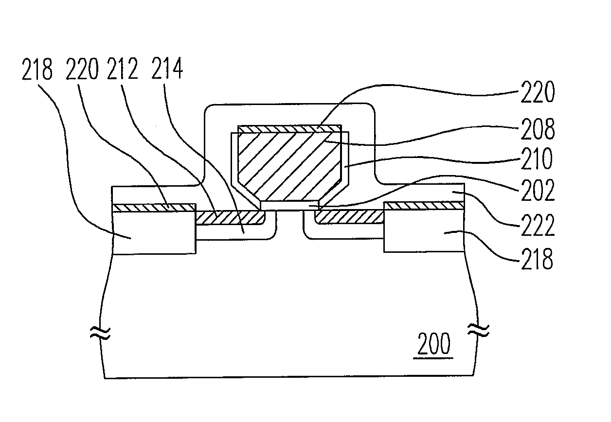
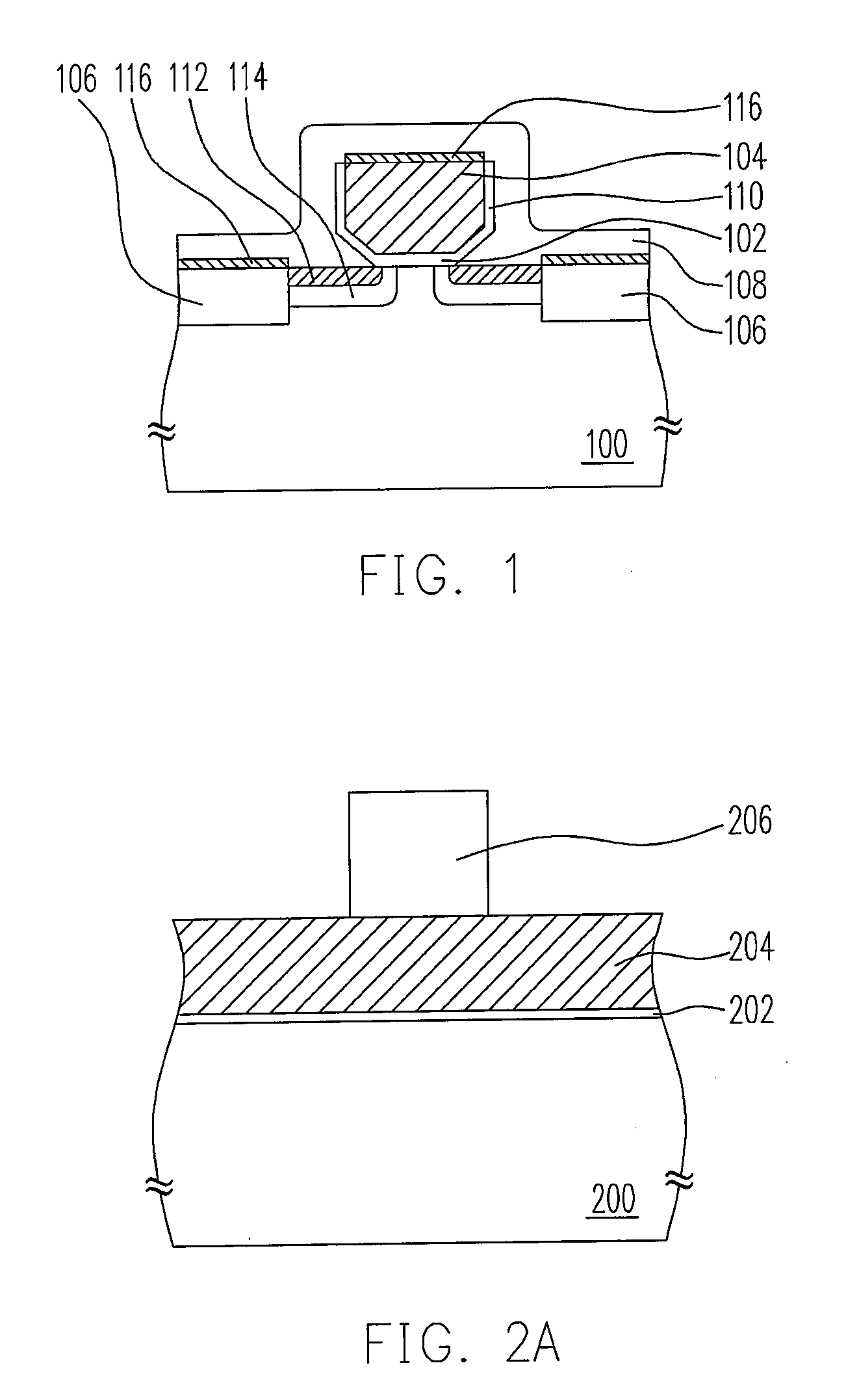
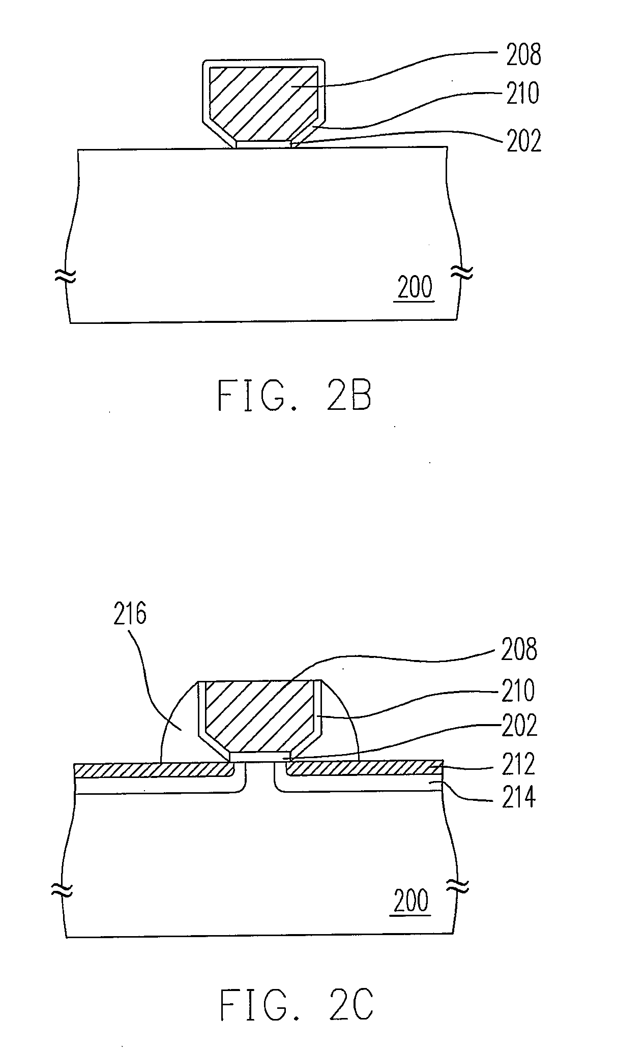
[0039]FIG. 1 is a schematic cross-sectional view of a semiconductor device according to one embodiment of the present invention. As shown in FIG. 1, the semiconductor device is an NMOS transistor, for example. The semiconductor device comprises a semiconductor substrate 100, a gate dielectric layer 102, a gate 104, a pair of source / drain regions 106, a stressed layer 108, a liner oxide layer 110, a lightly doped region 112, a halo implant region 114 and a metal silicide layer 116.

[0040] The semiconductor substrate 100 is a silicon substrate or a SOI substrate, for example. The gate dielectric layer 102 is disposed on the semiconductor substrate 100 and fabricated using silicon oxide, for example.

[0041] The...


PUM


Abstract

A method of fabricating a semiconductor device is provided herein. The semiconductor device includes a substrate, a gate dielectric layer, a gate, a pair of source / drain regions and a stressed layer. The gate dielectric layer is disposed on the substrate and the gate whose top area is larger than its bottom area is disposed on the gate dielectric layer. The source / drain regions are disposed in the substrate next to the sidewalls of the gate. The stressed layer is disposed on the substrate to cover the gate and the source / drain regions.

Description

CROSS-REFERENCE TO RELATED APPLICATION [0001] This application is a divisional of an application Ser. No. 11 / 308,390, filed Mar. 21, 2006, now pending. The entirety of each of the above-mentioned patent application is hereby incorporated by reference herein and made a part of this specification.BACKGROUND OF THE INVENTION [0002] 1. Field of the Invention [0003] The present invention relates to a semiconductor device and fabricating method thereof. More particularly, the present invention relates to a semiconductor device and fabricating method thereof that can improve the operating efficiency of the semiconductor device by controlling partial mechanical stress. [0004] 2. Description of the Related Art [0005] In semiconductor production, the dimensions of semiconductor devices are often reduced to attain a higher operating speed and a lower power consumption. However, with the ever-increasing level of integration of devices, the miniaturization of the devices has almost reached a lim...

Claims


Application Information

Patent Timeline
Patent Type & Authority Applications(United States)
IPC IPC(8): H01L21/336
CPCH01L21/28114H01L21/31116H01L21/32137H01L21/823807H01L29/7843H01L29/42376H01L29/665H01L29/6653H01L29/7833H01L21/823864
Inventor CHANG, HUI-CHENLIN, TONYHSU, BROOKCHEN, CYRUS LWLEE, MENG-LINSHIAU, WEI-TSUN
Owner UNITED MICROELECTRONICS CORP
Why Eureka
Try Eureka