Three-dimensional memory device incorporating segmented array line memory array

a memory array and three-dimensional technology, applied in semiconductor devices, digital storage, instruments, etc., can solve the problems of increasing the power dissipation by a factor of n, affecting the overall capacitance of the bit line during sensing, etc.

Active Publication Date: 2007-11-15
WODEN TECH INC
View PDF70 Cites 47 Cited by
  • Summary
  • Abstract
  • Description
  • Claims
  • Application Information

AI Technical Summary

Benefits of technology

[0007] In certain embodiments, the present invention provides a three-dimensional (3D) high density memory array with array lines that can be short in at least one direction, by having multiple layers of segmented bit lines (e.g., sense lines) with segment switch devices within the memory array that connect the segments to global bit lines. The segment switch devices reside on one or more layers of the integrated circuit, preferably residing on each bit line layer. The global bit lines reside preferably on one layer below the memory array, but in some embodiments may reside on more than one layer. In some embodiments, the bit line segments share vertical connections to an associated global bit line. The capacitance per unit length of the global bit line is lower than that of the bit line segments because the global bit line does not bear the capacitance of unselected bit line segments, and thus the overall capacitance of the bit line during sensing is reduced because only one of the many segmented bit lines associated with a given column is coupled to the global bit line.
[0008] The overall resistance of the combined bit line may also be reduced because the global bit line may be implemented having a larger pitch than the bit line segments, and also may be implemented using a lower resistance material than the usually much shorter segmented bit lines that may be implemented using a material having a relatively high resistance per unit length. This invention also provides for a 3D memory array which reduces power consumption by segmenting the memory array lines in at lease one direction into small pieces, thereby partitioning the array into many small array blocks, only one of which needs to be fully active.
[0009] In some embodiments, the present invention provides a three-dimensional electrically erasable read-only memory (EEROM) array by means of an arrangement of multiple layers of segmented bit lines with segment connection switches on multiple layers and shared vertical connections to a global bit line layer. Such memory arrays may be realized with much less write-disturb effects for half selected memory cells (i.e., those coupled to either the selected word line or selected bit line segment, but not both), and may be realized with a much smaller block of cells to be erased.
[0012] There are many reasons for very high density memories to limit the length of the memory array sense lines. In DRAM arrays, it is desirable to limit the bit line capacitance. In FeRAM arrays, it is desirable to limit the capacitance of bit lines and the capacitance of the capacitor plate line. In diode-isolated matrix arrays, such as diode-antifuse (AF) memory arrays, it is desirable to reduce the number of reverse biased diode leakage paths. Each of these types of memory cells may be implemented into a memory array in accordance with one or more embodiments of the present invention to achieve an improved and more efficient 3D memory array.

Problems solved by technology

These vertical connections cannot lie beneath the individual memory cells on each layer, and thus may add significantly to the chip area.
But a large fan-out frequently has certain electrical disadvantages depending on the memory cell technology being used.
For example, the capacitance of array lines and the resistance of array lines may increase by the fan-out (N) factor, and leakage per cell may cause power dissipation to increase by a factor of N2.
This interaction is detrimental for EEPROM arrays because it causes a partial, but cumulative, disturb of some bits while reading or writing other bits.
Because the number of half-selected cells increases with increasing fan-out, and because the amount a cell is disturbed is a cumulative effect of a great number of cycles (which varies with fan out proportional to N2), the data in those cells could easily be destroyed if the array line fan-outs were large.
As a result, 3D memory arrays must make a fan-out trade-off between electrical requirements and layout efficiency that is particularly detrimental in 3D EEPROM arrays.

Method used


Image

  • Three-dimensional memory device incorporating segmented array line memory array
  • Three-dimensional memory device incorporating segmented array line memory array
  • Three-dimensional memory device incorporating segmented array line memory array

Examples


Embodiment Construction

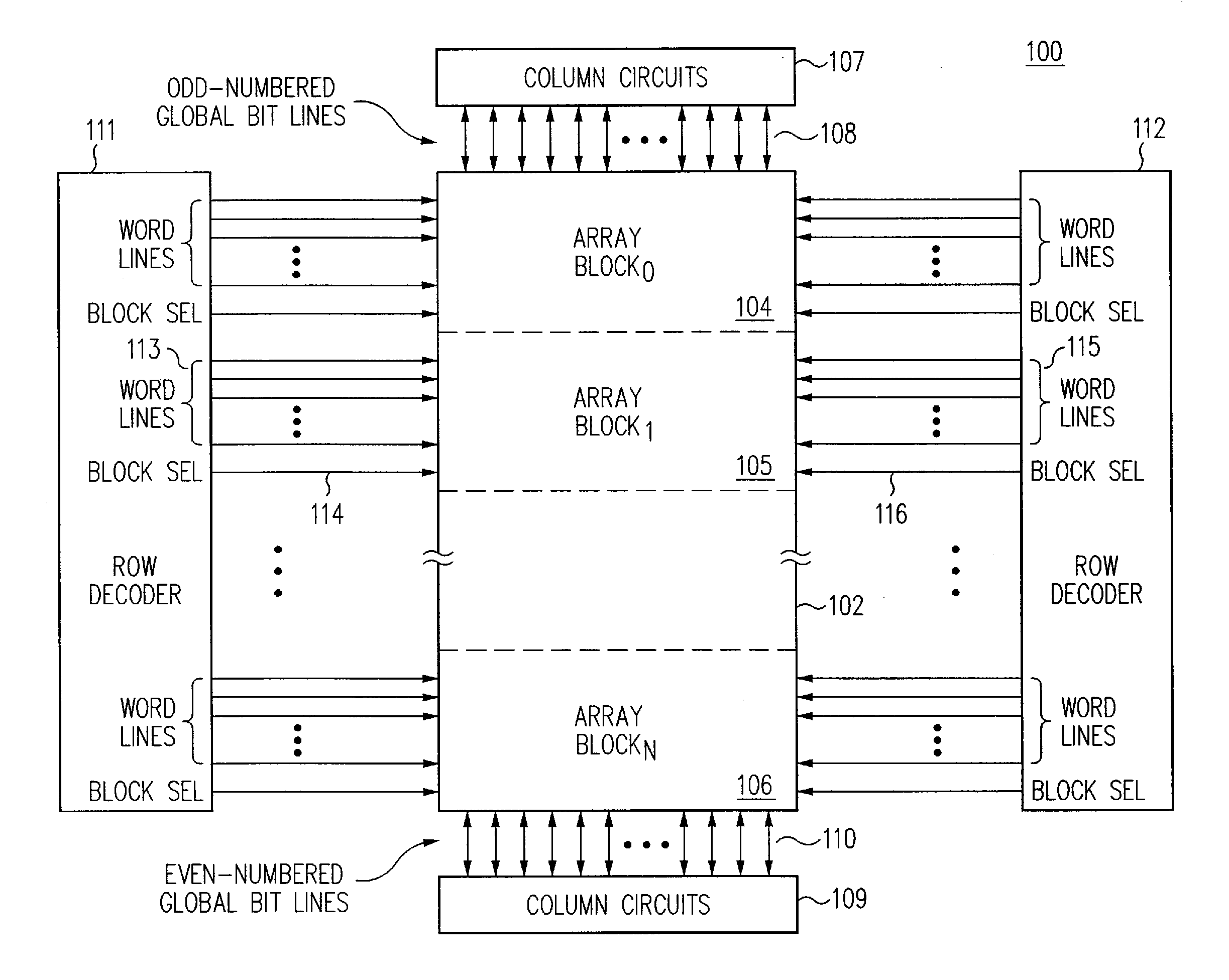
[0032] Referring now to FIG. 1, a block diagram is depicted of an exemplary memory array organization 100 including a memory array 102 having a plurality of array blocks 104, 105, . . . 106. Half of the word lines for each array block are driven by a row decoder 111 to the left of the array102, while the other half of the word lines for each array block are driven by a row decoder 112 to the right of the array 102. Using array block 105 as an example, a group of word lines 113 is provided by the row decoder 111 (which may represent the even-numbered word lines), while a second group of word lines 115 is provided by the row decoder 112 (which may represent the odd-numbered word lines). The row decoder 111 also provides one or more block select signals 114 to the array block 105, while the row decoder 112 also provides one or more block select signals 116 to the array block 105.

[0033] The memory array 102 includes a plurality of global bit lines, described further below. Half of the ...


PUM


Abstract

A three-dimensional (3D) high density memory array includes multiple layers of segmented bit lines (i.e., sense lines) with segment switch devices within the memory array that connect the segments to global bit lines. The segment switch devices reside on one or more layers of the integrated circuit, preferably residing on each bit line layer. The global bit lines reside preferably on one layer below the memory array, but may reside on more than one layer. The bit line segments preferably share vertical connections to an associated global bit line. In certain EEPROM embodiments, the array includes multiple layers of segmented bit lines with segment connection switches on multiple layers and shared vertical connections to a global bit line layer. Such memory arrays may be realized with much less write-disturb effects for half selected memory cells, and may be realized with a much smaller block of cells to be erased.

Description

CROSS-REFERENCE TO RELATED APPLICATION(S) [0001] This application is a continuation application of co-pending U.S. application Ser. No. 10 / 403,752 by Roy E. Scheuerlein, et al, entitled “Three-Dimensional Memory Device Incorporating Segmented Bit Line Memory Array”, filed on Mar. 31, 2003, which application is hereby incorporated by reference in its entirety.FIELD OF THE INVENTION [0002] The present invention relates to semiconductor integrated circuits containing memory arrays, and in preferred embodiments the invention particularly relates to monolithic three-dimensional memory arrays. BACKGROUND [0003] Recent developments in semiconductor processing technologies and memory cell technologies have continued to increase the density achieved in integrated circuit memory arrays. For example, certain passive element memory cell arrays may be fabricated having word lines approaching the minimum feature size (F) and minimum feature spacing for the particular word line interconnect layer,...

Claims


Application Information

Patent Timeline
Patent Type & Authority Applications(United States)
IPC IPC(8): G11C5/06G11C7/18G11C11/06G11C11/4097G11C16/04G11C17/12G11C17/18H01L31/0328
CPCG11C7/18G11C16/0416G11C16/0466Y10S257/91G11C17/18G11C2213/71G11C2213/77G11C17/12
Inventor SCHEUERLEIN, ROY E.ILKBAHAR, ALPERFASOLI, LUCAG
Owner WODEN TECH INC
Why Eureka
Try Eureka