Plasma display panel driving circuit and plasma display apparatus

a technology of driving circuit and display panel, which is applied in the direction of instruments, color television details, television systems, etc., can solve the problems of increasing forward voltage drop, increasing the loss of recovery circuit of semiconductor elements, and serious problems of parasitic components, so as to reduce the number of elements connected in parallel, the effect of reducing the resistance reducing the loss of the protective diod

Inactive Publication Date: 2007-11-22
PANASONIC CORP
View PDF9 Cites 40 Cited by
  • Summary
  • Abstract
  • Description
  • Claims
  • Application Information

AI Technical Summary

Benefits of technology

[0024] According to the invention, in the power recovery circuit, when the counterflow preventive diode element is switched from ON state to OFF state by the protective diode, a closed current channel including recovery inductor and recovery switch element is formed, and the voltage applied to the protective diode is reduced, and the withstand voltage of the protective diode can be lowered. As a result, loss of protective diode is decreased, the number of elements connected in parallel can be reduced, and the mounting area can be decreased.
[0025] Further, the invention also suppresses the surge voltage generated when the counterflow preventive diode is changed from ON state to OFF state, and the withstand voltage of counterflow preventive diode can be lowered, and normal bias voltage drop Vf of counterflow preventive diode is lowered, and the recovery rate of electric power accumulated in the capacitive load of plasma display panel is improved, and the power consumption can be saved.

Problems solved by technology

Effects of such parasitic components are serious problems when the diode element is switched from ON to OFF state.
Elevation of withstand voltage between terminals leads to increase of semiconductor element loss of recovery circuit such as increase of forward voltage drop and decline of switching speed.
In configuration of semiconductor elements, there are various limits from the aspects of substrate area, heat releasing efficiency of cooling plates for fixing semiconductor elements, and others, and it is practically next to impossible to design thick and short wiring pattern while satisfying these limits, and it has been difficult to keep the parasitic inductance always at low level.
Moreover, since the loss of semiconductor elements is increased, a plurality of semiconductor elements must be connected in parallel, which causes to increase the cost and increase the mounting area.

Method used


Image

  • Plasma display panel driving circuit and plasma display apparatus
  • Plasma display panel driving circuit and plasma display apparatus
  • Plasma display panel driving circuit and plasma display apparatus

Examples


Embodiment Construction

[0040] A preferred embodiment of the invention is described specifically below by referring to the accompanying drawings.

1. PDP Driving Circuit

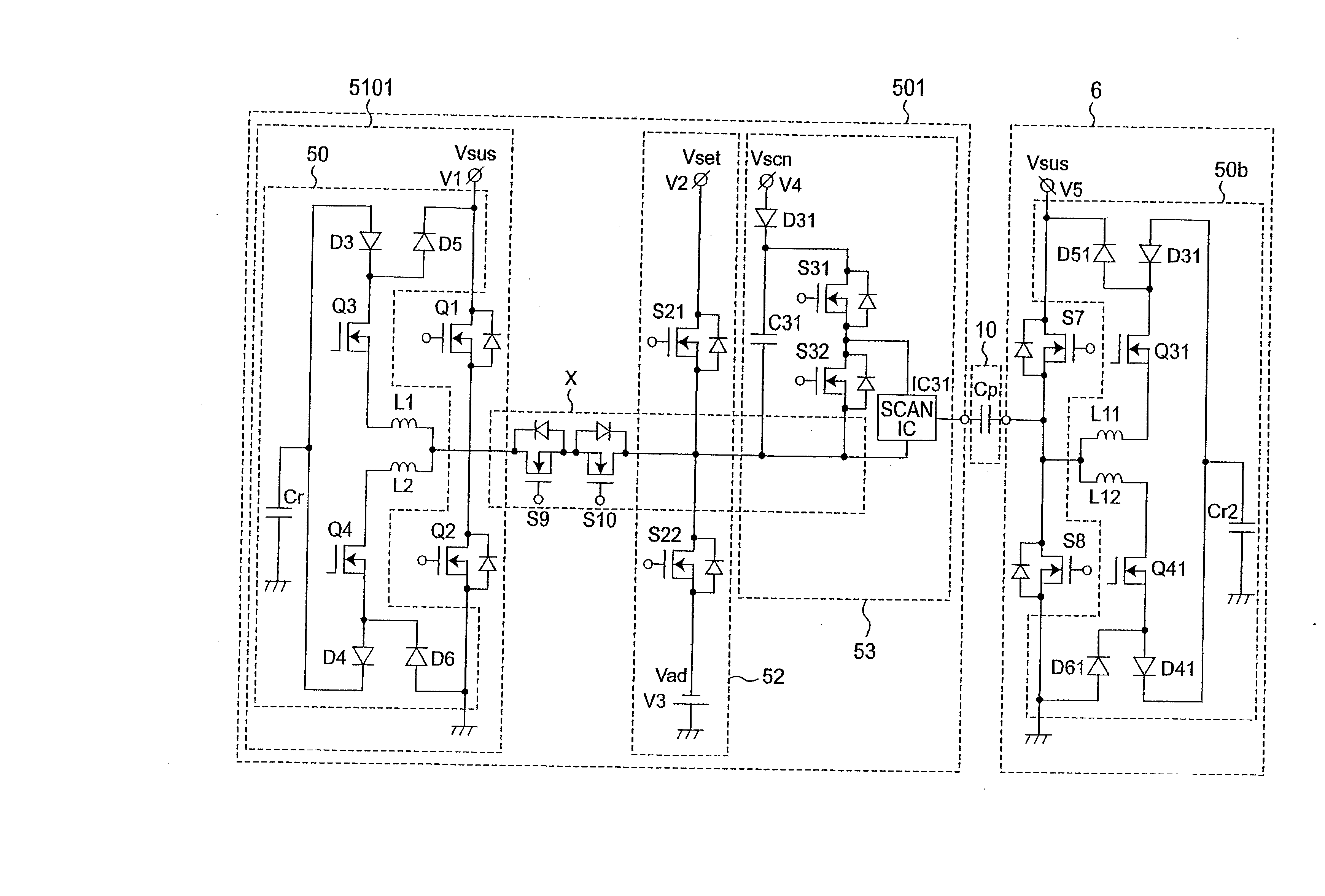
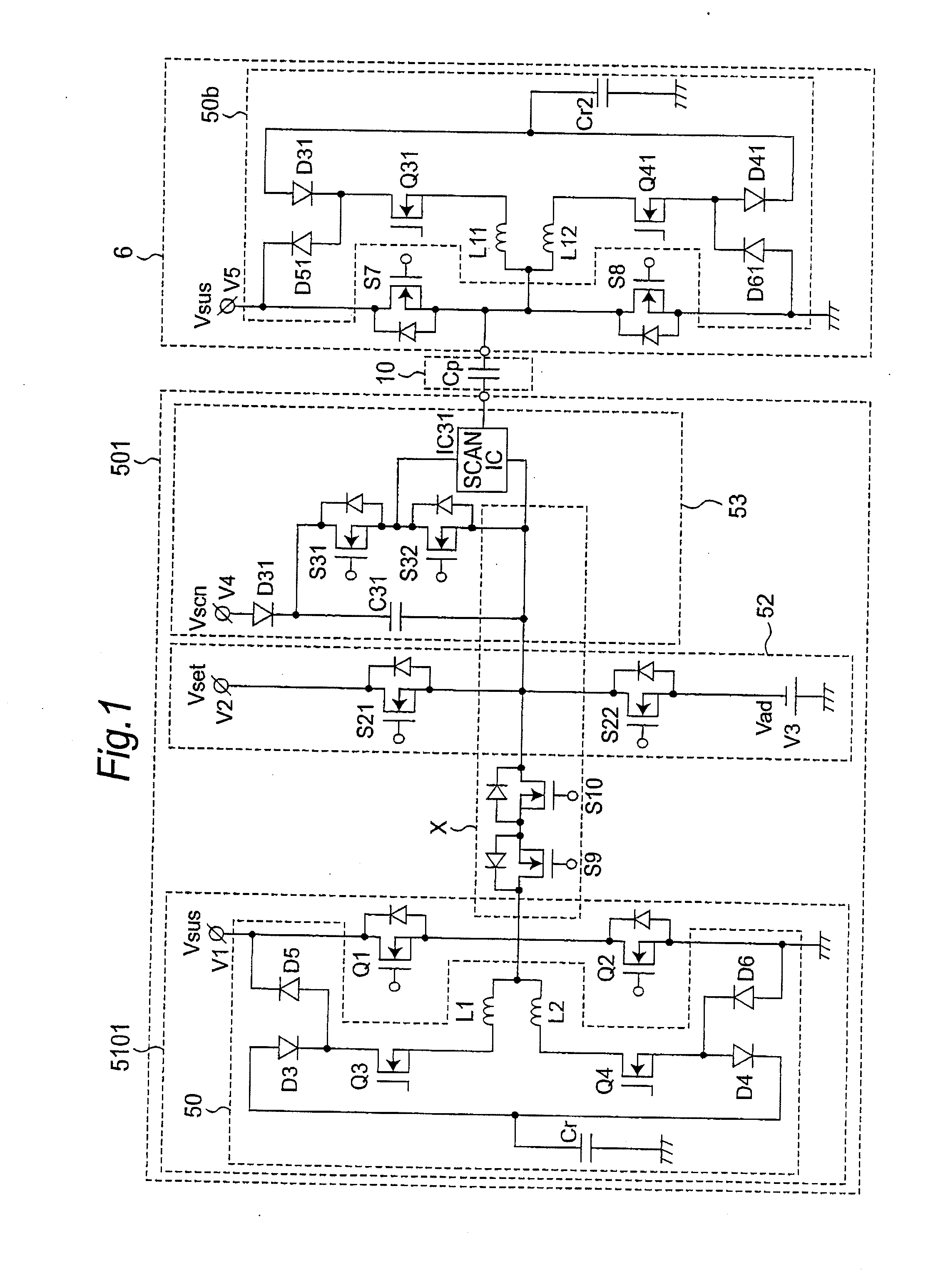
[0041]FIG. 1 is a block diagram of PDP driving circuit in an embodiment of the invention. The PDP driving circuit shown in FIG. 1 is a circuit for applying a drive voltage to electrodes of a plasma display panel (PDP), and driving the PDP. Prior to specific description of configuration and operation of PDP driving circuit, the configuration and operation of PDP are explained below. In FIG. 1, the PDP 10 is shown as a capacitive addition Cp.

1.1 Plasma Display Panel (PDP)

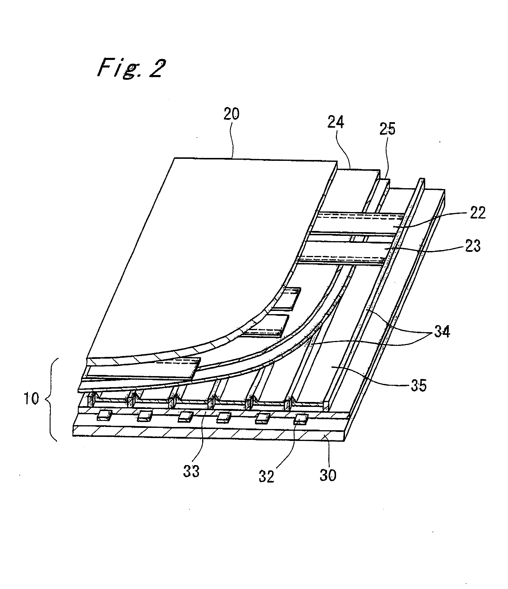
[0042]FIG. 2 is a perspective view that indicates a structure of plasma display panel (PDP) driven by the PDP driving circuit of the embodiment. On a glass front plate 20 which is a first substrate, a plurality of display electrodes are formed in a pair of stripe scan electrode 22 and stripe sustain electrode 23. To cover the scan electrode 22 and sustain electrode 23, a di...


PUM


Abstract

A PDP driving circuit is comprised of a power recovery unit for recovering an electric power from a capacitive load by resonance operation with PDP which is the capacitive load Cp, and reusing the recovered power. The power recovery unit includes a recovery inductor for resonating with the capacitive load, a recovery switch element for connecting the recovery capacitor to the capacitive load and recovery inductor, and forming a channel for passing resonance current, a counterflow preventive diode for blocking flow of current in the recovery switch element in reverse polarity direction, and a protective diode for forming a closed current channel including the recovery inductor and recovery switch element when the counterflow preventive diode is changed from ON state to OFF state.

Description

BACKGROUND OF THE INVENTION [0001] 1. Field of the Invention [0002] The present invention relates to a plasma display panel driving circuit, as well as plasma display apparatus, used for wall-mounted television sets and large-screen monitors. [0003] 2. Related Art [0004] An alternating-current surface discharge type plasma display panel (hereinafter called “PDP”) as a typical AC type is constituted by arranging a front plate containing a glass substrate formed by disposing a scan electrode and a sustain electrode which carry out surface discharge and a back plate containing a glass substrate formed by disposing data electrodes oppositely in parallel so that both electrodes set up a matrix and that a discharge space is formed in a gap, and by sealing the perimeter portion with sealing materials such as glass frit. Between both substrates of the front plate and the back plate, discharge cells divided by bulkheads area provided, and in a cell space between these bulkheads, a phosphor l...

Claims


Application Information

Patent Timeline
Patent Type & Authority Applications(United States)
IPC IPC(8): G09G3/28G09G3/20G09G3/288G09G3/291G09G3/294G09G3/296G09G3/298H04N5/66
CPCG09G2330/025G09G3/2965
Inventor ARAI, YASUHIROINOUE, MANABUNAGAKI, TOSHIKAZU
Owner PANASONIC CORP
Why Eureka
Try Eureka