Semiconductor-on-diamond devices and associated methods

a technology of semiconductors and diamonds, applied in semiconductor devices, semiconductor/solid-state device details, electrical apparatus, etc., can solve the problems of increased noise, increased lattice matching, and increased lattice thickness, so as to improve lattice matching

Active Publication Date: 2007-11-22
SUNG CHIEN MIN
View PDF11 Cites 22 Cited by
  • Summary
  • Abstract
  • Description
  • Claims
  • Application Information

AI Technical Summary

Benefits of technology

[0012]Various steps can further be taken to improve the lattice matching between the Si substrate and the base layer. For example, in one aspect a layer of SiC may be deposited onto the lattice-orienting Si substrate s...

Problems solved by technology

In addition to the tremendous density issues that already exist, with the current movement toward size reduction, ULSI is becoming even more delicate, both in size and materials than ever before.
As current technology moves beyond ULSI, several barriers emerge that may be insurmountable with current wafer and substrate materials.
One barrier arises due to the accumulation of heat that may not be effectively channeled out of the crystal lattice of Group IV semiconductors.
However, as the power requirements future generations of semiconductor devices increase, copper heat spreaders will become reservoirs for heat accumulation.
Accumulation of the carriers creates noise, and tends to obscure...

Method used


Image

  • Semiconductor-on-diamond devices and associated methods
  • Semiconductor-on-diamond devices and associated methods
  • Semiconductor-on-diamond devices and associated methods

Examples


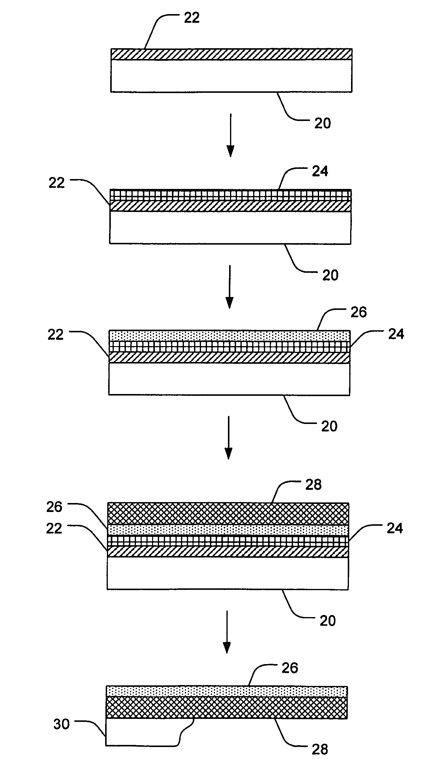
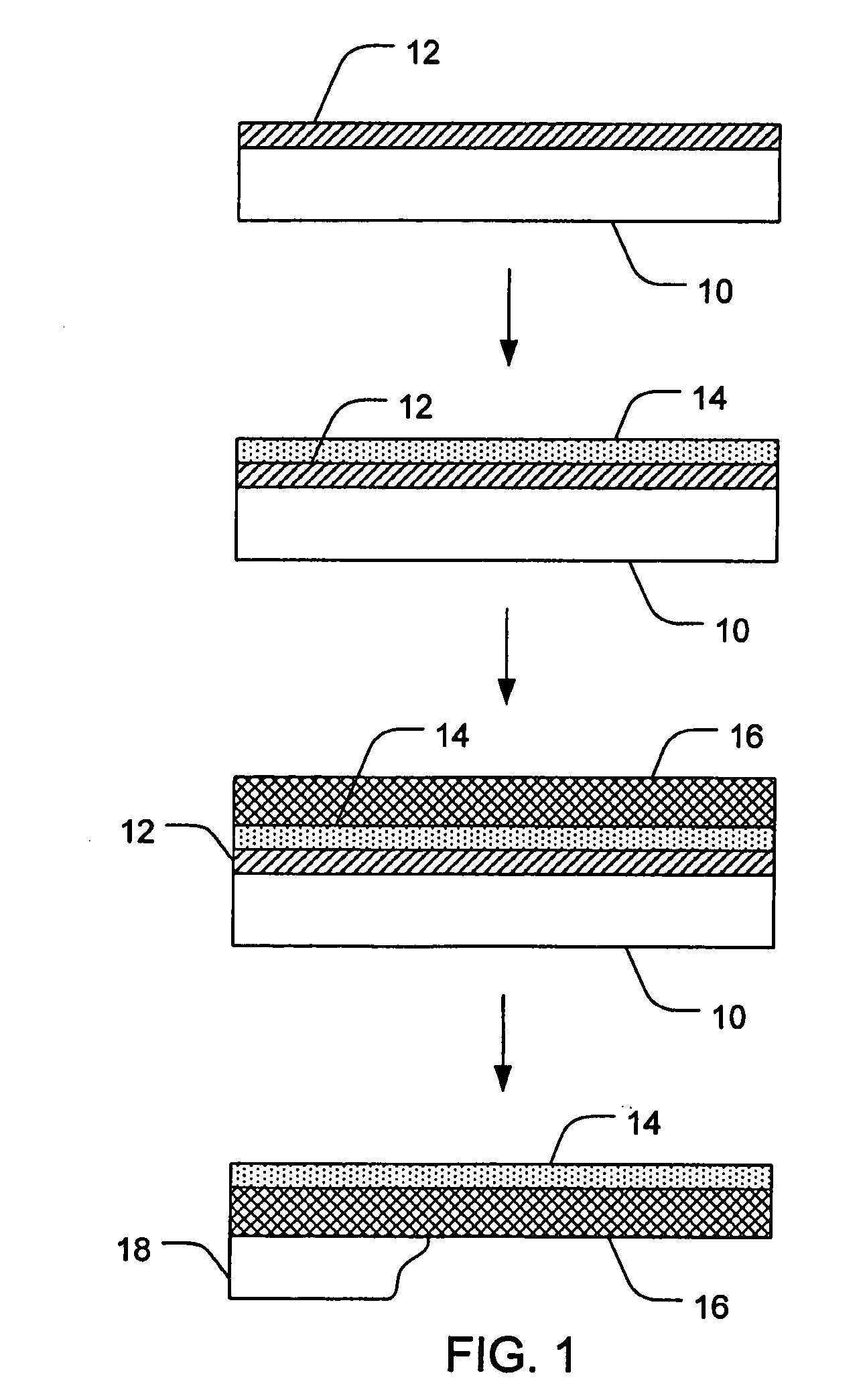
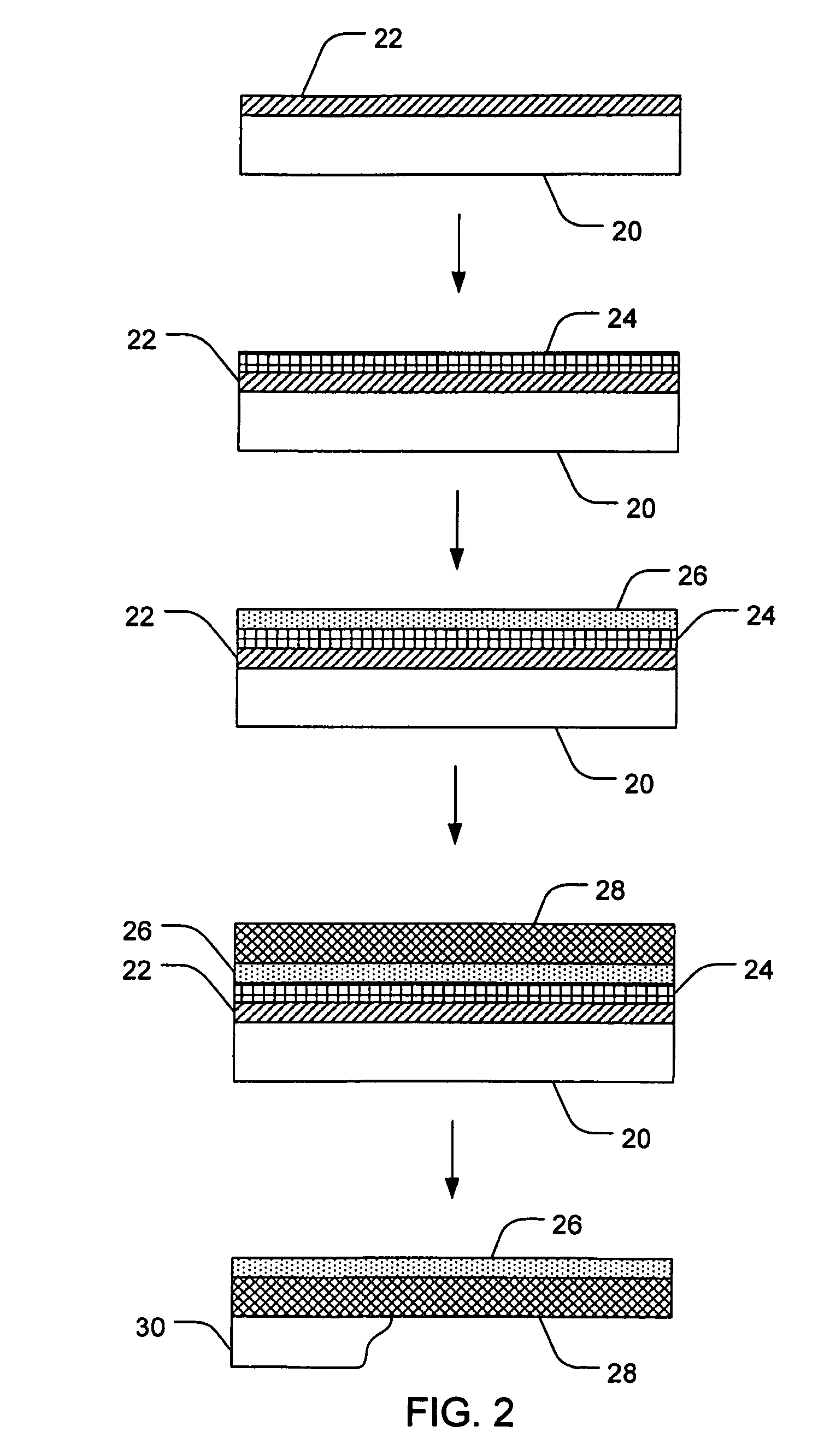
Embodiment Construction

[0019]Before the present invention is disclosed and described, it is to be understood that this invention is not limited to the particular structures, process steps, or materials disclosed herein, but is extended to equivalents thereof as would be recognized by those ordinarily skilled in the relevant arts. It should also be understood that terminology employed herein is used for the purpose of describing particular embodiments only and is not intended to be limiting.

[0020]It must be noted that, as used in this specification and the appended claims, the singular forms “a,” and, “the” include plural referents unless the context clearly dictates otherwise. Thus, for example, reference to “an intermediate layer” includes one or more of such layers, reference to “a carbon source” includes reference to one or more of such carbon sources, and reference to “a CVD technique” includes reference to one or more of such CVD techniques.

Definitions

[0021]In describing and claiming the present inve...


PUM


Abstract

Semiconductor-on-diamond (SOD) substrates and methods for making such substrates are provided. In one aspect, a method of making an SOD substrate may include depositing a base layer onto a lattice-orienting silicon (Si) substrate such that the base layer lattice is substantially oriented by the Si substrate, depositing a semiconductor layer onto the base layer such that the semiconductor layer lattice is substantially oriented with respect to the base layer lattice, and disposing a layer of diamond onto the semiconductor layer. The base layer may include numerous materials, including, without limitation, aluminum phosphide (AlP), boron arsenide (BAs), gallium nitride (GaN), indium nitride (InN), and combinations thereof. Additionally, the method may further include removing the lattice-orienting Si substrate and the base layer from the semiconductor layer. In one aspect, the Si substrate may be of a single crystal orientation.

Description

FIELD OF THE INVENTION[0001]The present invention relates generally to methods of making substrates having a semiconductor layer disposed on a diamond substrate, as well as associated devices. Accordingly, the present invention involves the chemical and material science fields.BACKGROUND OF THE INVENTION[0002]As computers and other electronic devices become smaller and faster, the demands placed on semiconductor devices utilized therein increase geometrically. Ultra-large-scale integration (ULSI) is a technology that places at least 1 million circuit elements on a single semiconductor chip. In addition to the tremendous density issues that already exist, with the current movement toward size reduction, ULSI is becoming even more delicate, both in size and materials than ever before. As current technology moves beyond ULSI, several barriers emerge that may be insurmountable with current wafer and substrate materials.[0003]One barrier arises due to the accumulation of heat that may no...

Claims


Application Information

Patent Timeline
IPC IPC(8): H01L21/20
CPCH01L21/02381H01L21/02433H01L2924/0002H01L21/02439H01L21/02458H01L21/02488H01L21/02502H01L21/02505H01L21/0251H01L21/02527H01L23/3732H01L33/007H01L33/0079H01L2924/00H01L33/0093
Inventor SUNG, CHIEN-MIN
Owner SUNG CHIEN MIN
Why Eureka
Try Eureka