Method of manufacturing semiconductor device

a manufacturing method and semiconductor technology, applied in the manufacturing of semiconductor/solid-state devices, basic electric elements, electric devices, etc., can solve the problems of not being able to completely sublime the product, peeling of the barrier metal film at the side surfaces of the connection holes, etc., to reduce the variations of electrical characteristics of the connection hole portion, the reliability and manufacturing yield of the semiconductor device can be improved, and the effect of reducing the variation of electrical characteristics

Active Publication Date: 2007-11-22
RENESAS ELECTRONICS CORP
View PDF7 Cites 102 Cited by
  • Summary
  • Abstract
  • Description
  • Claims
  • Application Information

AI Technical Summary

Benefits of technology

[0029]Since it is possible to reduce variations of electrical characteristics in connecti...

Problems solved by technology

However, there are various kinds of technological problems explained below in the above dry cleaning treatment.
When the product remains, there arise problems such as variations of contact resistance between the barrier metal film and the conductive material thereunder at the bottoms of the ...

Method used


Image

  • Method of manufacturing semiconductor device
  • Method of manufacturing semiconductor device
  • Method of manufacturing semiconductor device

Examples


first embodiment

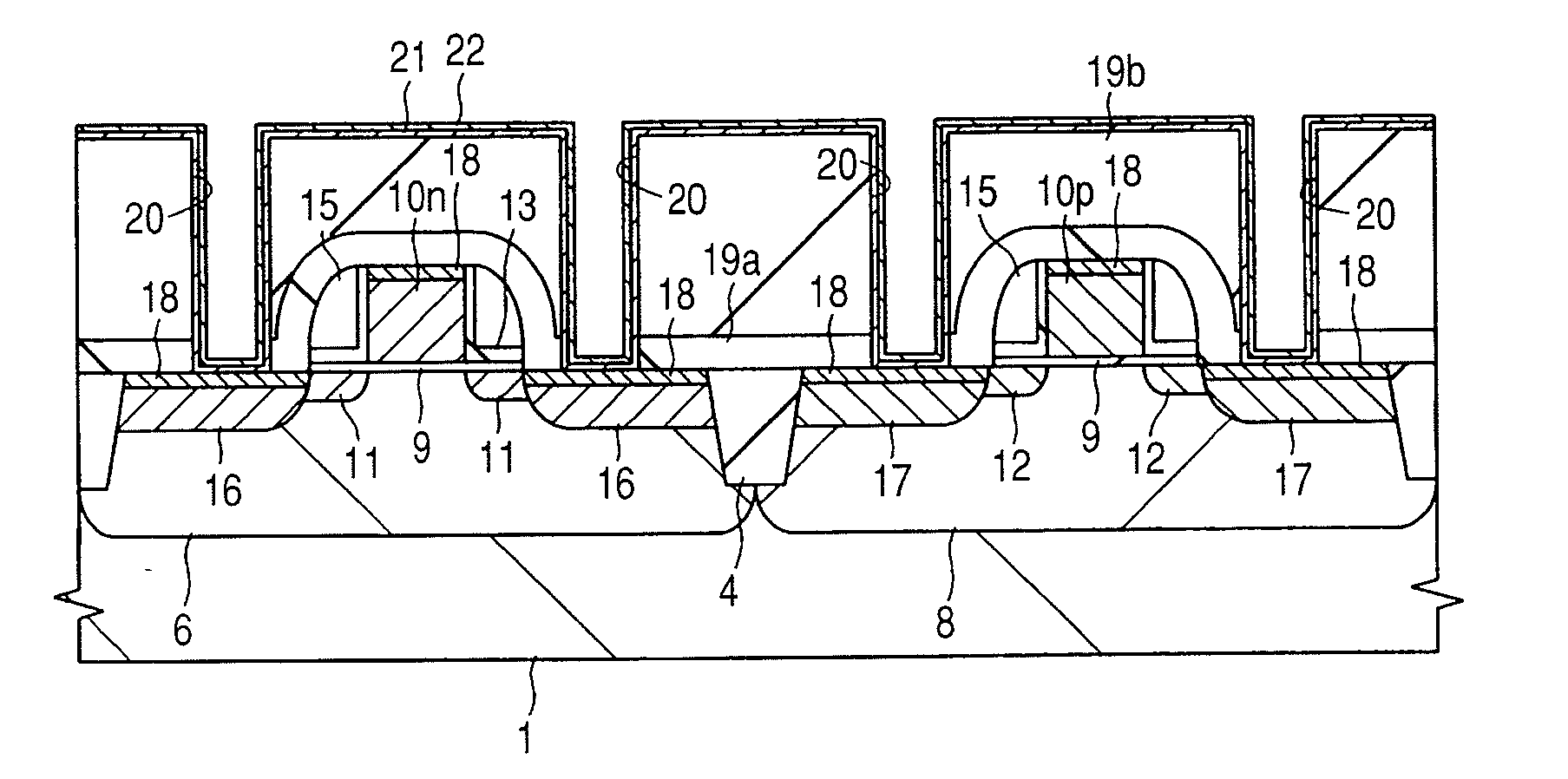
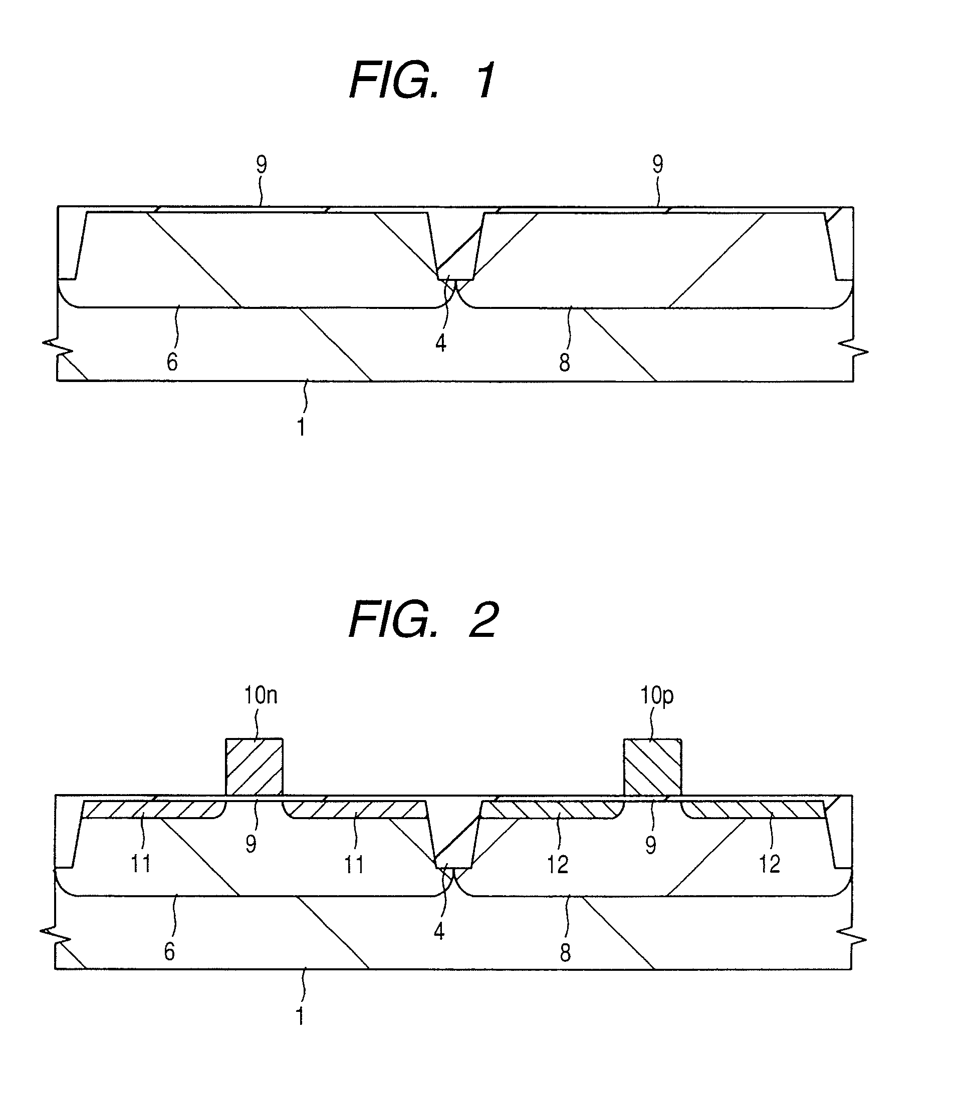
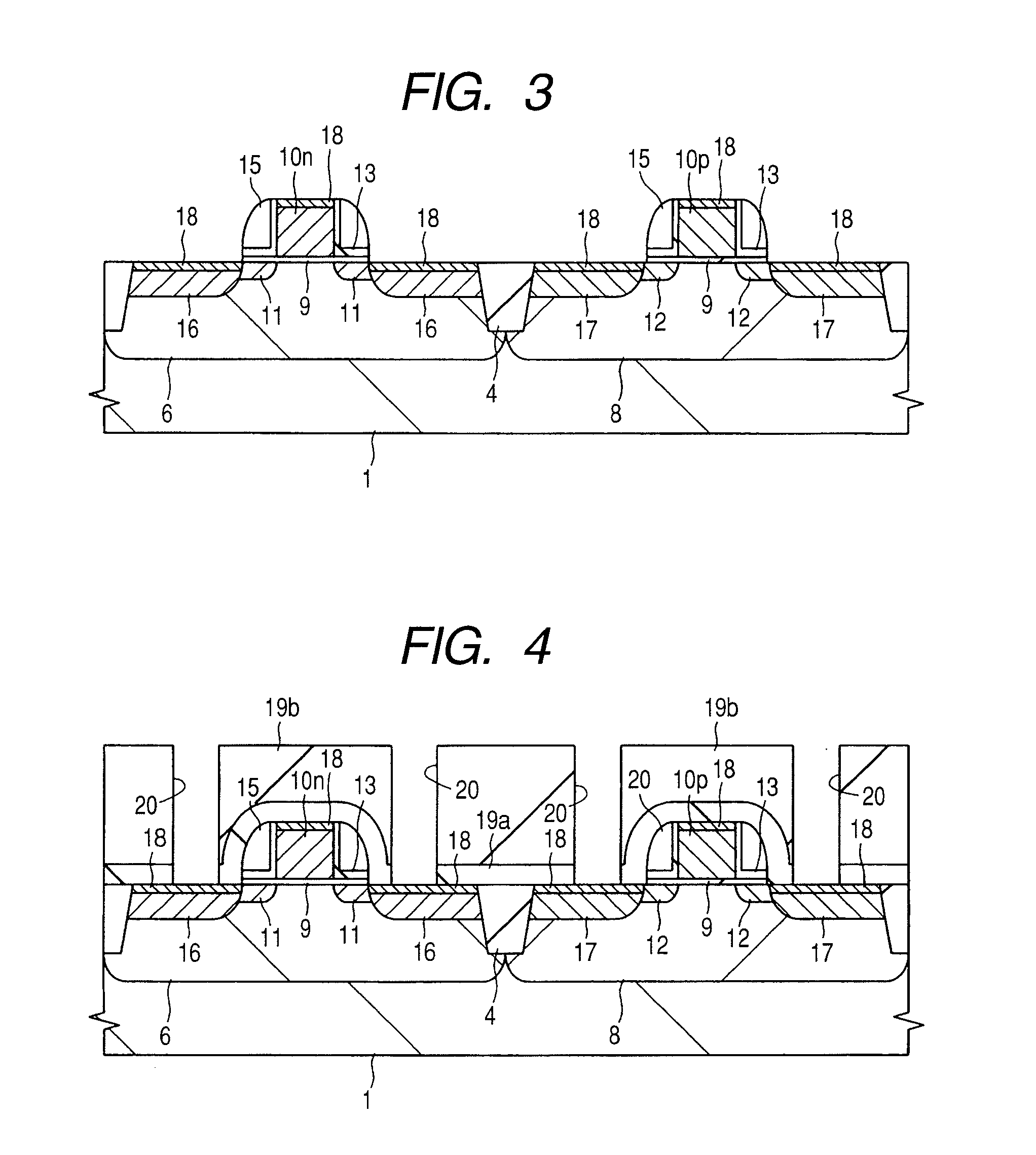
[0051]A method of manufacturing a CMOS (Complementary Metal Oxide Semiconductor) device according to a first embodiment of the invention will be explained with reference to FIG. 1 to FIG. 14. FIG. 1 to FIG. 5A and FIG. 5B, and FIG. 11 to FIG. 14 show cross-sectional views of relevant parts of the CMOS device, FIG. 6 is a schematic plan view of a barrier-metal deposition system, FIG. 7 is a chart of deposition steps of the barrier-metal film, FIG. 8 is a schematic cross-sectional view of a chamber for dry cleaning treatment provided in the barrier metal deposition system, FIGS. 9A, 9B and 9C respectively show schematic cross-sectional views of the chamber for explaining processing steps of a semiconductor wafer in the chamber for dry cleaning treatment provided in the barrier-metal film deposition system, and FIG. 10 is a graph showing the relation between electric current flowing in a gate electrode and a semiconductor substrate, and the heat treatment temperature in the case that d...

second embodiment

[0099]As explained in the first embodiment, in the dry cleaning treatment performed in the process of forming the barrier metal film, the product remains at the principal surface and parts of the side surface and the rear surface of the semiconductor wafer SW. Consequently, the product having a composition of (NH4)2SiF6 is removed by heating the semiconductor wafer SW at a temperature of 100 to 150° C., using the showerhead 57c set to 180° C., which is provided in the chamber 57 for dry cleaning treatment, further, the product of a composition which is slightly different from (NH4)2SiF6 is removed by heating the semiconductor wafer SW at the temperature higher than 150° C. by the chambers 55, 56 for heating treatment.

[0100]In a second embodiment of the invention, the temperature of a showerhead 57CH provided in the chamber 57 for dry cleaning treatment is set to a temperature higher than 180° C., for example, at 250° C., and the semiconductor wafer SW is heated at a temperature at 1...

third embodiment

[0110]As described in the embodiment, in the dry cleaning treatment performed in the step of forming the barrier metal film, the semiconductor wafer SW is merely put over the wafer stage 57a in general, therefore, the product having the composition of (NH4)2SiF6 remains not only at the principal surface of the semiconductor wafer SW but also at parts of the side surface and the rear surface of the semiconductor wafer SW. The product remaining at parts of the side surface and the rear surface of the semiconductor wafer SW peels off when the semiconductor wafer SW is transferred to another chamber and other occasions, which causes dirt or dust. Consequently, in the first and second embodiments, heat treatment is performed to the semiconductor wafer SW in the same chamber 57, continued from the dry cleaning treatment, thereby removing the product remaining at the principal surface of the semiconductor wafer SW as well as the product remaining at parts of the side surface and the rear s...


PUM


Abstract

To provide a technology capable of improving reliability and manufacturing yield of a semiconductor device by reducing variations of electrical characteristics in connection hole portions. After a semiconductor wafer is placed over a wafer stage provided in a chamber for dry cleaning treatment of a deposition system, dry cleaning treatment is performed to a principal surface of the semiconductor wafer by supplying reducing gas, sequentially, heat treatment is performed to the semiconductor wafer at a first temperature of 100 to 150° C. by a showerhead which is maintained at 180° C. Next, after the semiconductor wafer is vacuum transferred from the chamber to a chamber for heat treatment, heat treatment is performed to the semiconductor wafer at a second temperature of 150 to 400° C. in the chamber, thereby removing a product remaining over the principal surface of the semiconductor wafer.

Description

CROSS-REFERENCE TO RELATED APPLICATIONS[0001]The disclosure of Japanese Patent Application No. 2006-138949 filed on May 18, 2006 including the specification, drawings and abstract is incorporated herein by reference in its entirety.BACKGROUND OF THE INVENTION[0002]The invention relates to a manufacturing technology of a semiconductor device, particularly, relates to a technology which is effective when applied to manufacturing processes of a semiconductor device in which a metal film is embedded into connection holes opened in an insulating film.BACKGROUND ART[0003]In Japanese Patent Application Laid-open No. 2003-324108 (corresponding to U.S. Pat. No. 6,864,183), a method of removing a natural oxide film existing at the surface of a silicon substrate and a gate electrode is enclosed, which is performed by plasma etching using mixed gas of argon gas and at least one or more kinds of fluoride gasses selected from a group including nitrogen trifluoride gas, hydrogen fluoride gas, two-...

Claims


Application Information

Patent Timeline
IPC IPC(8): H01L21/4763H01L21/44
CPCH01L21/02063H01L21/28518H01L21/2855H01L21/76846H01L21/67207H01L21/6831H01L21/76814H01L21/67069H01L21/28H01L21/304H01L21/324
Inventor FUTASE, TAKUYATOBIMATSU, HIROSHI
Owner RENESAS ELECTRONICS CORP
Why Eureka
Try Eureka