

Semiconductor nanocrystal-metal complex and method of preparing the same
a technology of semiconductor nanocrystals and complexes, which is applied in the direction of crystal growth process, polycrystalline material growth, chemistry apparatus and processes, etc., can solve the problems of poor reactivity of semiconductor nanocrystals, complicated overall process, and limited applicability of existing techniques, so as to improve reactivity
- Summary
- Abstract
- Description
- Claims
- Application Information
AI Technical Summary
Benefits of technology
Problems solved by technology
Method used
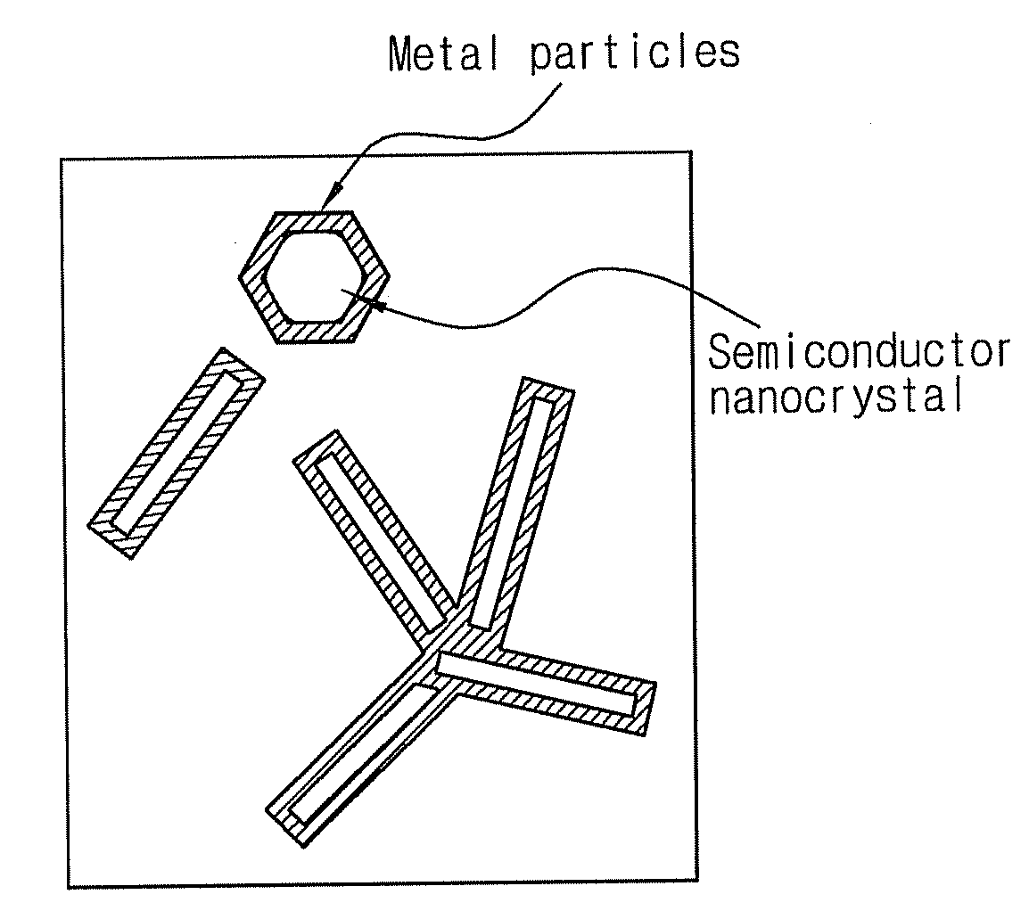
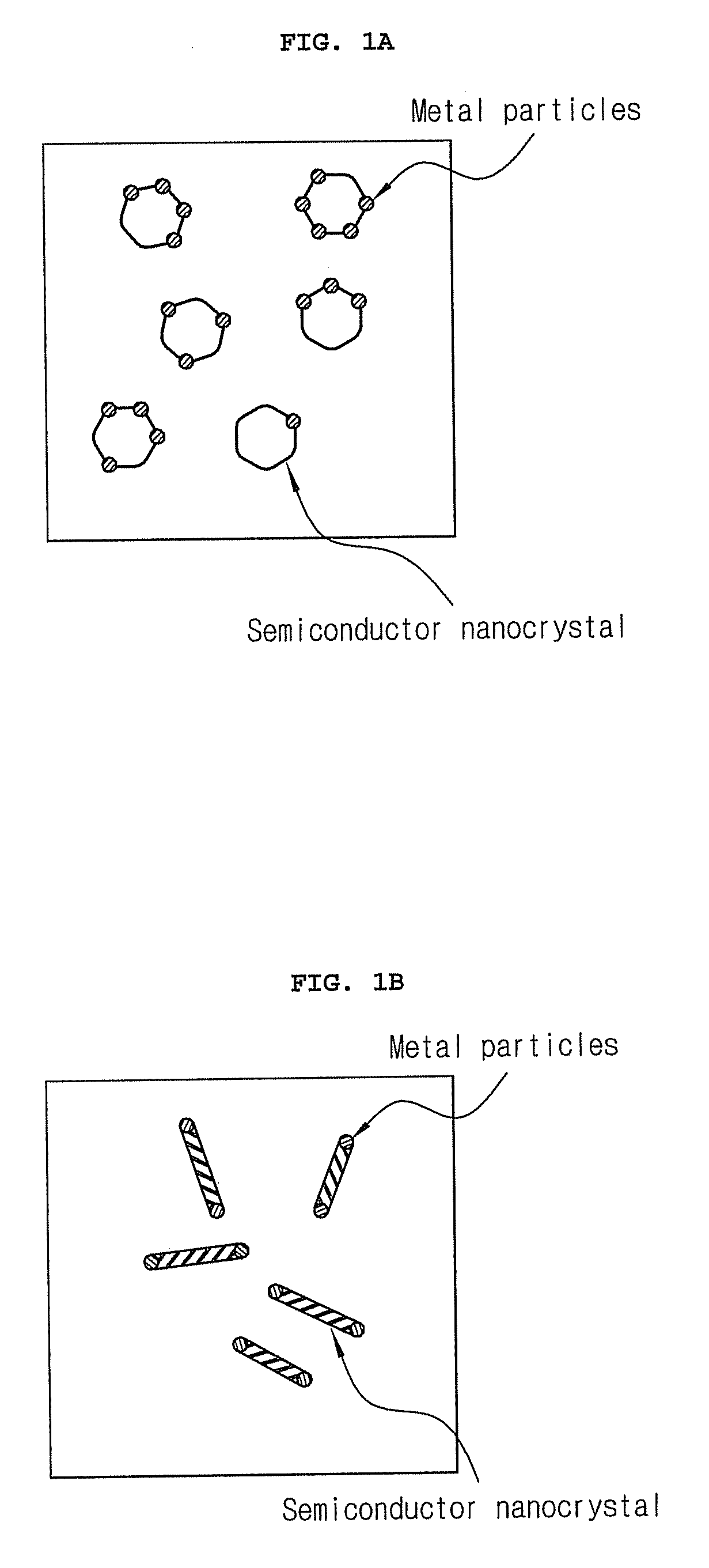
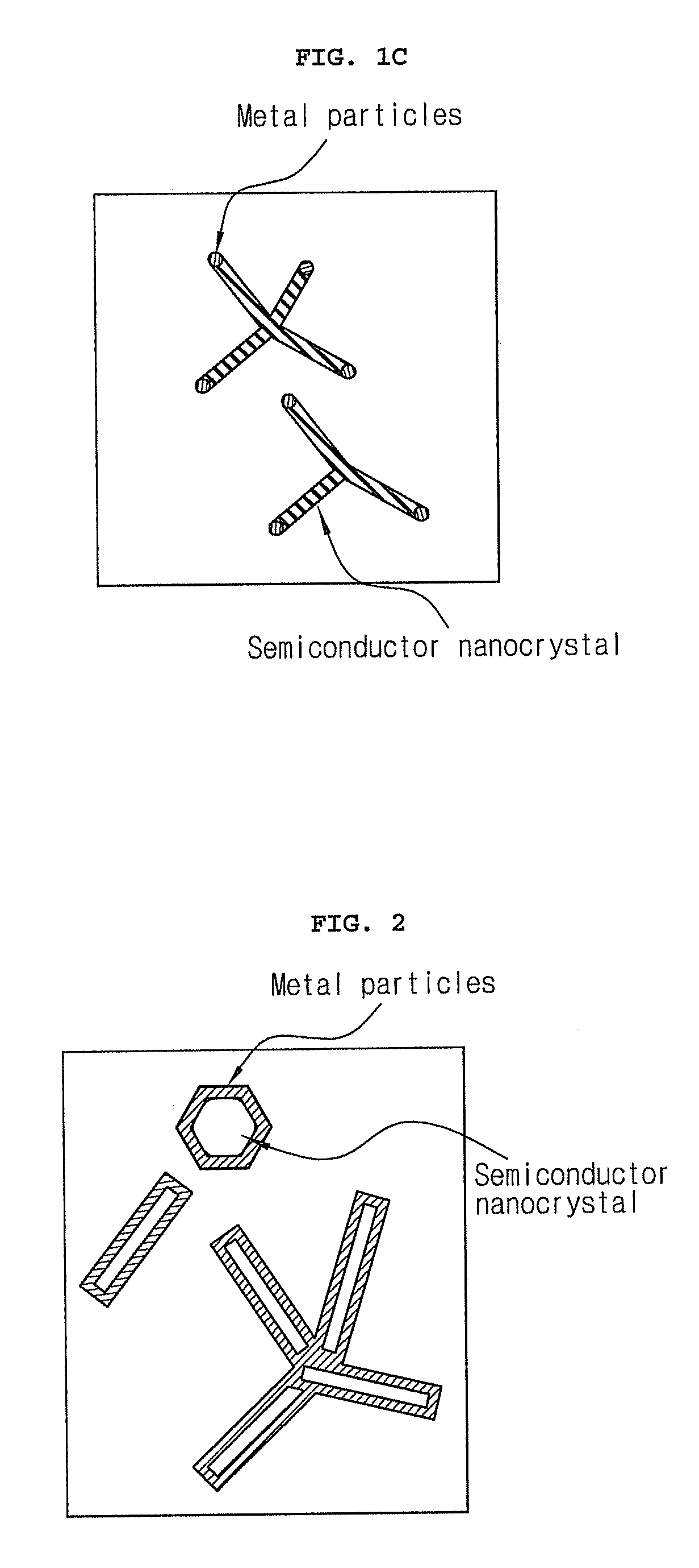
Image

Examples
example 1
Synthesis of Spherical Semiconductor Nanocrystal-Metal (CdSeS / Au) Complex
[0056]About 16 grams (g) of trioctylamine (TOA), about 0.5 g of oleic acid and about 0.4 millimoles (mmol) of cadmium oxide were simultaneously placed in a 100 milliliter (ml) flask equipped with a reflex condenser. The reaction temperature of the mixture was adjusted to about 300 degrees Celsius (° C.) with stirring to prepare a cadmium precursor solution. Separately, a selenium (Se) powder was dissolved in trioctylphosphine (TOP) to obtain an approximately 1 molar (M) Se-TOP complex solution, and a sulfur (S) powder was dissolved in TOP to obtain an approximately 0.4 M S-TOP complex solution.
[0057]A mixture of about 0.5 ml of the S-TOP complex solution and about 0.5 ml of the Se-TOP complex solution was rapidly fed to the cadmium precursor solution, followed by stirring for about 4 minutes to form a CdSeS nanocrystal or quantum dot (QD).
[0058]On the other hand, about 0.017 g of hydrogen tetrachloroaurate (HAu...
example 2
Synthesis of Bar-Shaped Semiconductor Nanocrystal-Metal (CdSe / Au) Complex
[0059]About 2.2 g of trioctylphosphine oxide (TOPO), about 1.07 g of octadecylphosphonic acid and about 0.205 g of cadmium oxide were simultaneously placed in a 100 ml-flask equipped with a reflex condenser. The reaction temperature of the mixture was adjusted to about 330° C. with stirring to prepare a cadmium precursor solution. Separately, about 0.063 g of a selenium (Se) powder, about 0.23 ml of tributylphosphine (TBT), about 1.74 ml of TOP and about 0.3 ml of toluene were mixed to obtain a Se complex solution. While the Se complex solution was fed to the cadmium precursor solution, the reaction temperature was lowered to about 280° C. The reaction mixture was stirred for about 6 minutes to form a bar-shaped CdSe nanocrystal.
[0060]Separately, about 0.017 g of hydrogen tetrachloroaurate (HAuCl4) was dissolved in THF, and then about 4 ml of OAm was added thereto to obtain a gold precursor solution. To the pre...
experimental example 1
Evaluation of Characteristics of Spherical Semiconductor Nanocrystal-Metal Complex
[0062]The characteristics of the spherical semiconductor nanocrystal-metal complex prepared in Example 1 were evaluated. After the spherical semiconductor nanocrystal-metal complex and the semiconductor nanocrystal quantum dot (QD) prepared in Example 1 were prepared, they were cooled to room temperature as rapidly as possible. Ethanol as a non-solvent was separately added to the nanocrystal-metal complex and the nanocrystal, and the resulting mixtures were centrifuged. The obtained precipitates were separated from the respective supernatants, and dispersed in toluene to prepare an about 1 wt % solution of the CdSeS nanocrystal and an about 1 wt % solution of the semiconductor nanocrystal-metal (CdSeS / Au) complex.
[0063]FIGS. 6 and 7 are absorption spectra and photoluminescence spectra of the CdSeS nanocrystal solution and the semiconductor nanocrystal-metal (CdSeS / Au) complex solution, respectively.
[00...
PUM
 Abstract
Description
Claims
Application Information