HYBRID INTEGRATION BASED ON WAFER-BONDING OF DEVICES TO AISb MONOLITHICALLY GROWN ON Si

a technology of monolithic aisb and integrated devices, which is applied in the direction of wave amplification devices, semiconductor lasers, electrical equipment, etc., can solve the problems of not being able to efficiently detect light, emit light, and si itself is not good optically active (i, optoelectronic) material

Active Publication Date: 2007-11-29
STC UNM
View PDF17 Cites 17 Cited by
  • Summary
  • Abstract
  • Description
  • Claims
  • Application Information

AI Technical Summary

Benefits of technology

[0007] According to various embodiments, the present teachings include a method for forming a semiconductor device. In this method, the semiconductor device can be formed by first forming an active-device structure including an active-device section formed on a III-V substrate, which can subsequently be thinned. A high-quality monolithic integration structure can then be formed through an interfacial misfit dislocation, wherein the high-quality monolithic integration structure can include a thinned III-V mating layer formed on a III-V nucleation layer formed on a silicon substrate. The thinned III-V substrate of the active-device structure can then be wafer-bonded onto the thinned III-V mating layer of the high-quality monolithic integration structure to form the semiconductor device.

Problems solved by technology

However, an intrinsic problem with integrating optoelectronics functionality into Si chips is that Si itself is not a good optically-active (i.e., optoelectronic) material as it neither emits nor detects light efficiently.
Due to the large lattice mismatch and thermal expansion coefficient mismatch between these materials and Si, monolithically integrated devices have been performance limited by the resulting crystalline defects (e.g., threading dislocations) from epitaxy.

Method used


Image

  • HYBRID INTEGRATION BASED ON WAFER-BONDING OF DEVICES TO AISb MONOLITHICALLY GROWN ON Si
  • HYBRID INTEGRATION BASED ON WAFER-BONDING OF DEVICES TO AISb MONOLITHICALLY GROWN ON Si
  • HYBRID INTEGRATION BASED ON WAFER-BONDING OF DEVICES TO AISb MONOLITHICALLY GROWN ON Si

Examples


Embodiment Construction

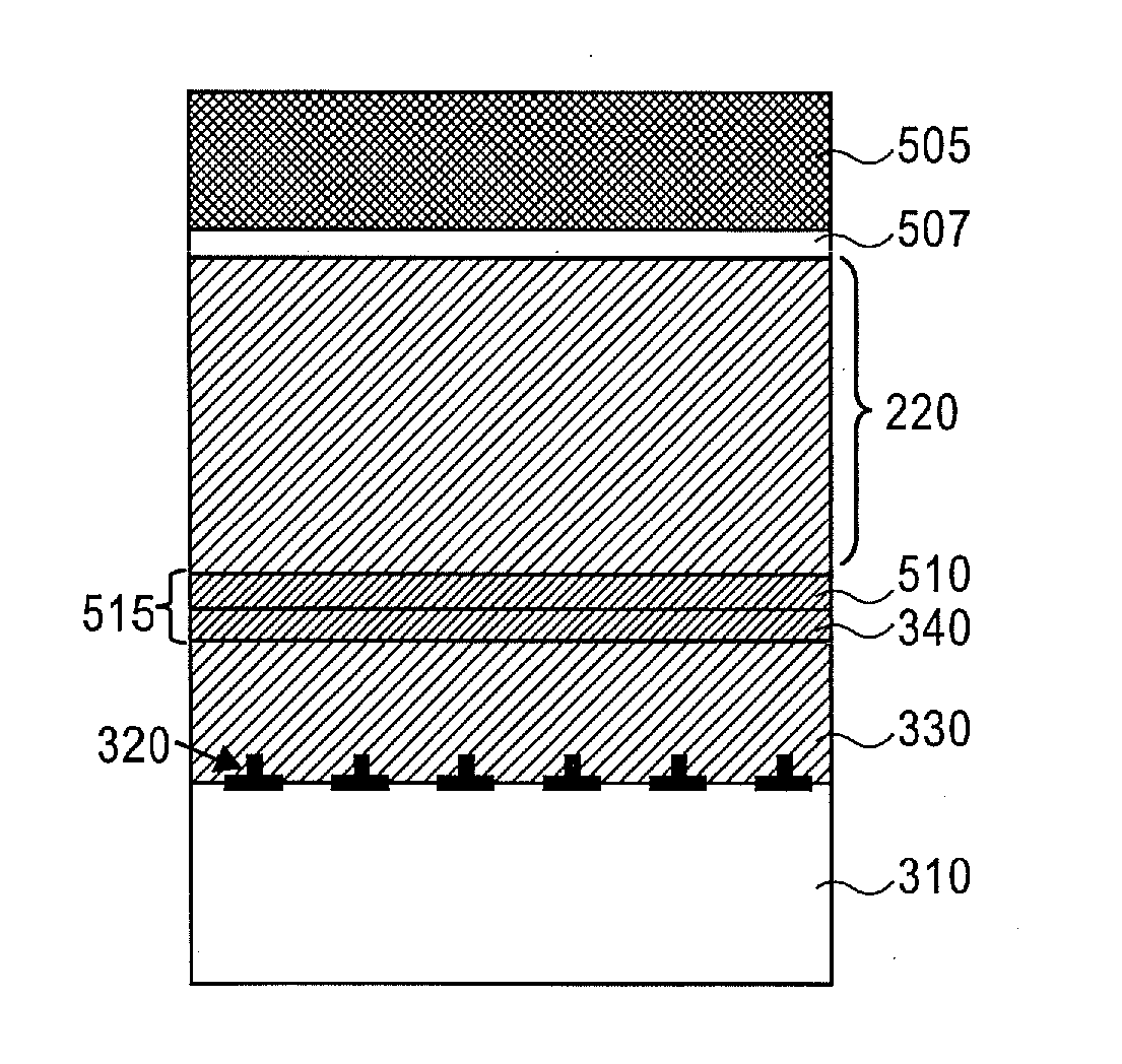
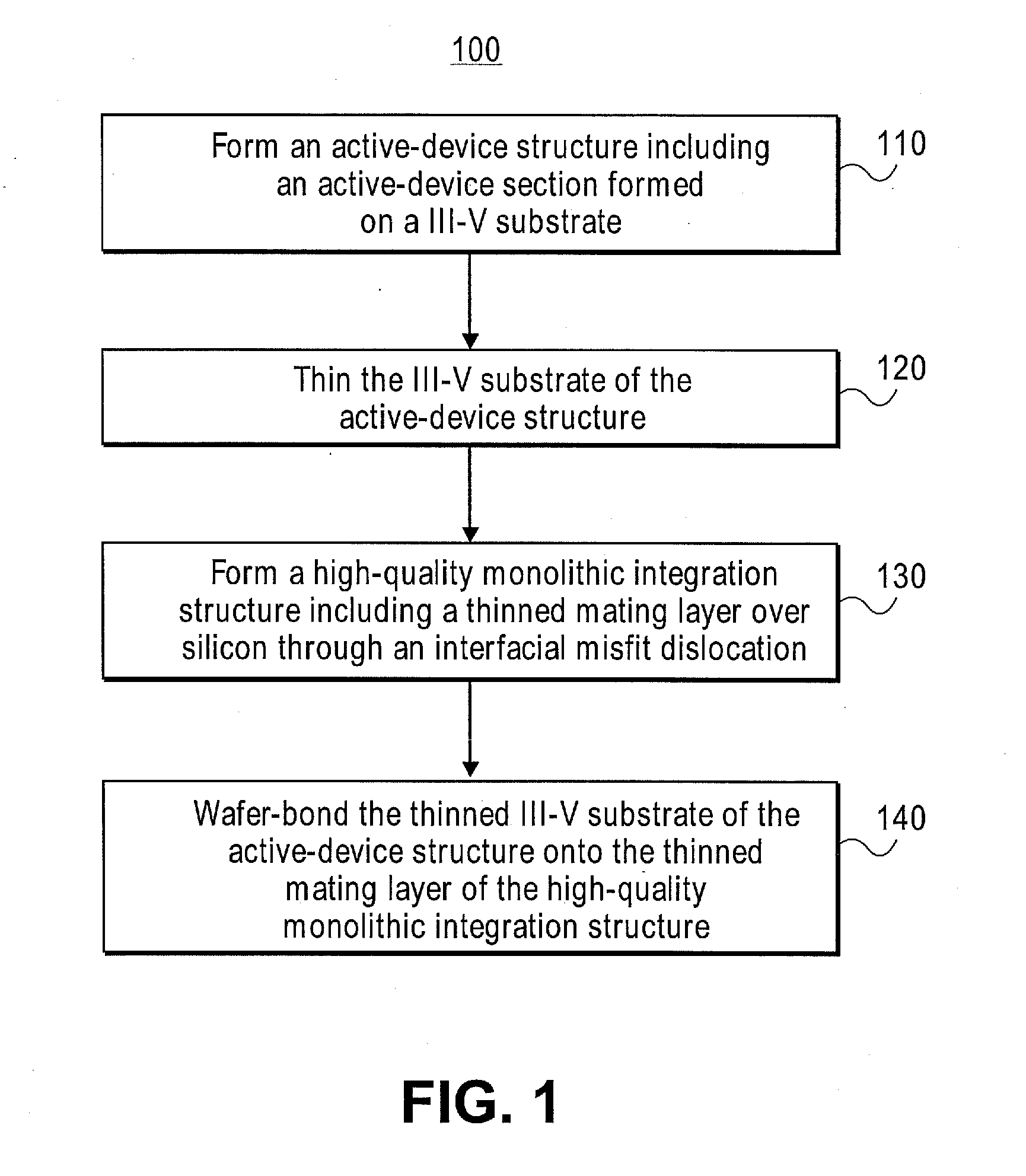
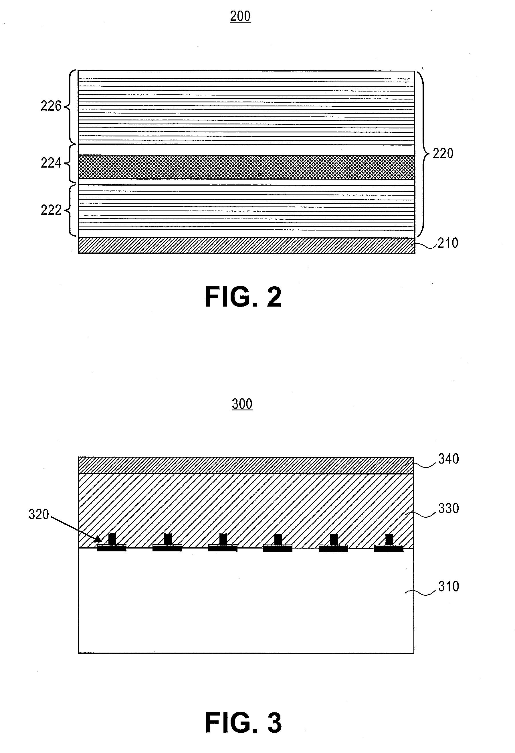
[0017] Reference will now be made in detail to the present embodiments (exemplary embodiments) of the invention, an example of which is illustrated in the accompanying drawings. Wherever possible, the same reference numbers will be used throughout the drawings to refer to the same or like parts. In the following description, reference is made to the accompanying drawings that form a part thereof, and in which is shown by way of illustration specific exemplary embodiments in which the invention may be practiced. These embodiments are described in sufficient detail to enable those skilled in the art to practice the invention and it is to be understood that other embodiments may be utilized and that changes may be made without departing from the scope of the invention. The following description is, therefore, merely exemplary.

[0018] While the invention has been illustrated with respect to one or more implementations, alterations and / or modifications can be made to the illustrated exam...


PUM


Abstract

Exemplary embodiments provide a semiconductor fabrication method including a combination of monolithic integration techniques with wafer bonding techniques. The resulting semiconductor devices can be used in a wide variety of opto-electronic and/or electronic applications such as lasers, light emitting diodes (LEDs), phototvoltaics, photodetectors and transistors. In an exemplary embodiment, the semiconductor device can be formed by first forming an active-device structure including an active-device section disposed on a thinned III-V substrate. The active-device section can include OP and/or EP VCSEL devices. A high-quality monolithic integration structure can then be formed with low defect density through an interfacial misfit dislocation. In the high-quality monolithic integration structure, a thinned III-V mating layer can be formed over a silicon substrate. The thinned III-V substrate of the active-device structure can subsequently be wafer-bonded onto the thinned III-V mating layer of the high-quality monolithic integration structure forming an optoelectronic semiconductor device on silicon.

Description

RELATED APPLICATIONS [0001] This application claims priority from U.S. Provisional Patent Application Ser. No. 60 / 757,869, filed Jan. 11, 2006, which is hereby incorporated by reference in its entirety.GOVERNMENT RIGHTS [0002] This invention was made with government support under Contract No. ZR 62J awarded by the Air Force Office of Scientific Research, and Contract No. ZR55N awarded by the Army Research Office. The government may have certain rights in the invention.FIELD OF THE INVENTION [0003] This invention relates generally to semiconductor devices and fabrication methods and, more particularly, to integrated devices and methods for device integration. BACKGROUND OF THE INVENTION [0004] It has been a long-standing desire of the microelectronics and telecommunications industries to combine optoelectronic components with silicon (Si) circuitry. A conventional solution for this combination includes a hybrid integration of optical components with Si integrated circuits (ICs). Howe...

Claims


Application Information

Patent Timeline
Patent Type & Authority Applications(United States)
IPC IPC(8): H01L21/46
CPCH01L21/187H01S5/183H01S5/028H01S5/0215
Inventor HUFFAKER, DIANA L.DAWSON, LARRY R.BALAKRISHNAN, GANESH
Owner STC UNM
Why Eureka
Try Eureka