

Formation method of metal layer on resin layer, printed wiring board, and producution method thereof
a technology of resin layer and metal layer, applied in the direction of conductive pattern formation, liquid/solution decomposition chemical coating, application, etc., can solve the problems of roughened shape, inverse interference with fine wiring formation, electric characteristics deterioration, etc., to suppress wiring dispersion and occurrence of defection, excellent electric properties
- Summary
- Abstract
- Description
- Claims
- Application Information
AI Technical Summary
Benefits of technology
Problems solved by technology
Method used
Image

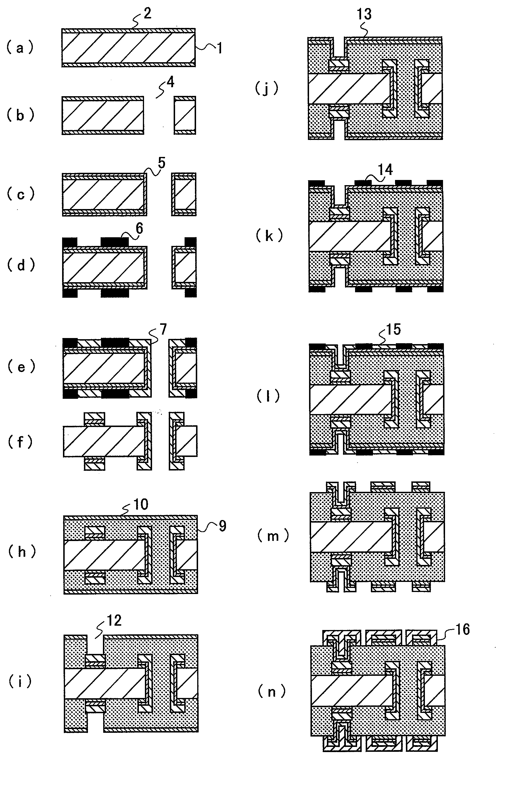
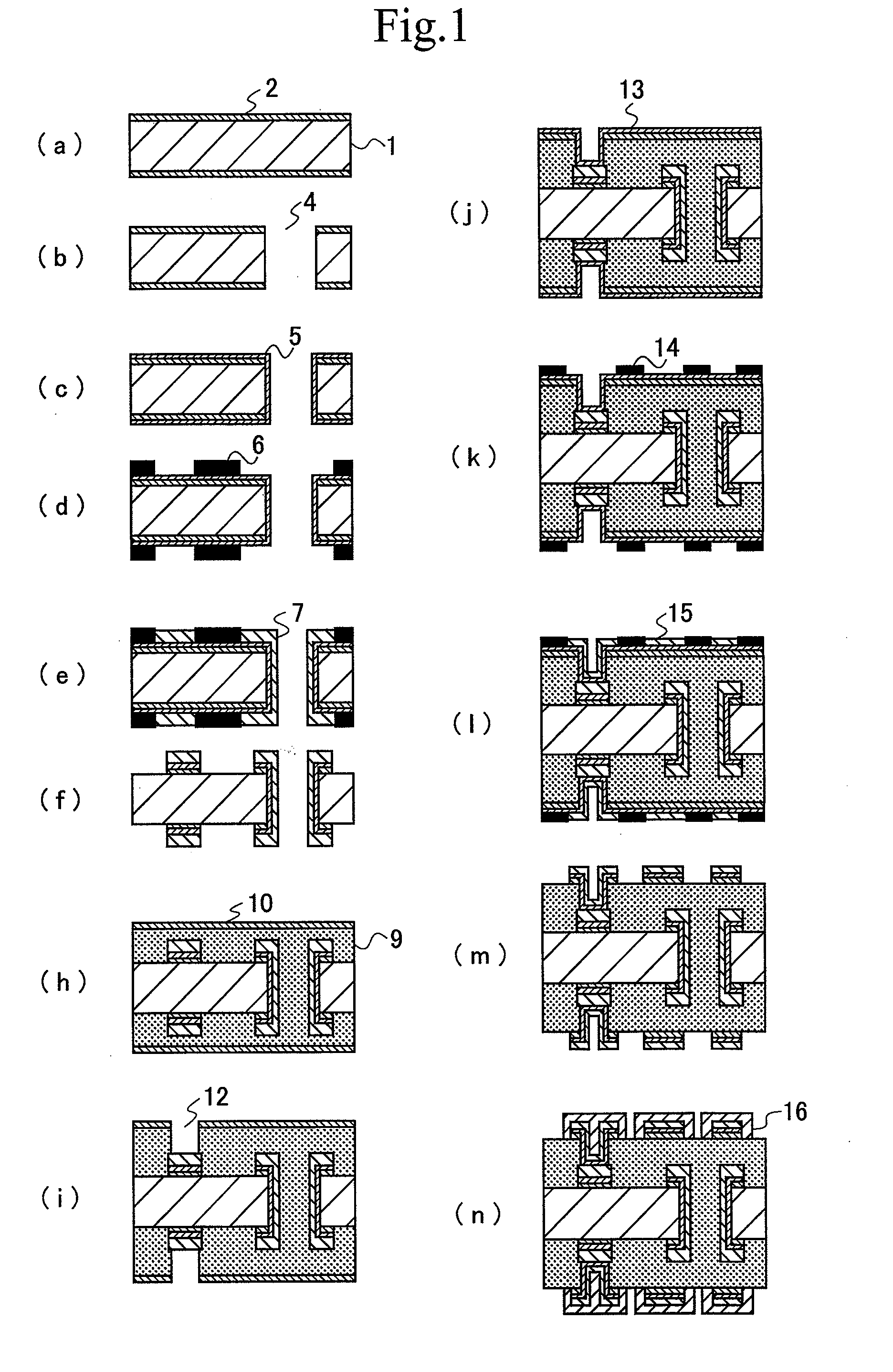
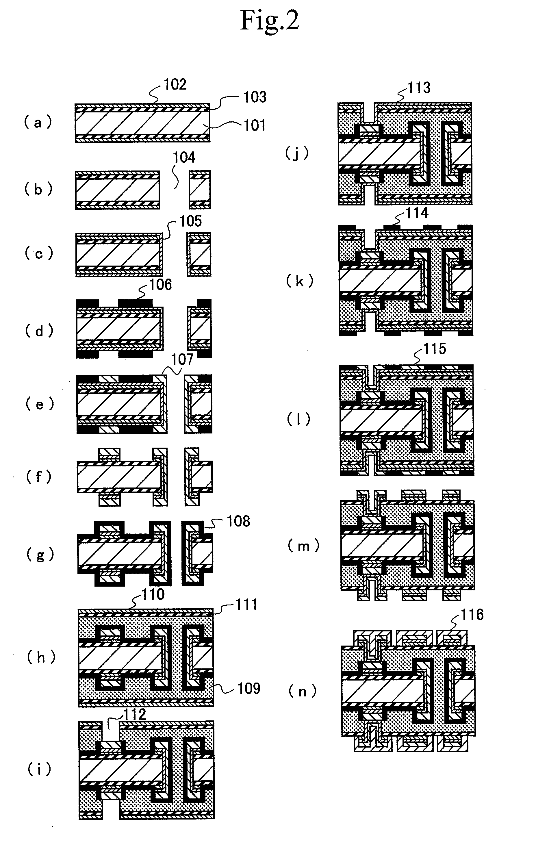
Examples
example 1a
[0138] The following metal foil A was produced.
Metal Foil A
[0139] Chromium plating was continuously carried out on the bright face of an electrolytic copper foil (a carrier copper foil) with a width of 510 mm and a thickness of 35 μm in the following conditions to form a chromium plating layer (a separation layer) with a thickness of 1.0 mg / dm2. The surface roughness (ten-point mean surface roughness) Rz after the chromium plating formation was 0.5 μm. The surface roughness was measured according to JIS-B-0601.
[0140] Solution composition: chromium trioxide 250 g / L and sulfuric acid 2.5 g / L,
[0141] Bath temperature: 25° C.,
[0142] Anode: lead, and
[0143] Electric current density: 20 A / dm2.
[0144] Next, electric copper plating in a thickness of 2.0 μm was carried out in the following bright conditions. The metal foil surface roughness Rz after the electric copper plating was 0.6 μm.
[0145] Solution composition: copper sulfate pentahydrate 100 g / L, sulfuric acid 150 g / L, and chlori...
example 1b
[0180] The following resin composition A was produced.
Resin Composition A
[0181] A separable flask 500 mL capacity equipped with a Deen / Stark refluxing cooling apparatus, a thermometer, and a stirrer was loaded with (4,4′-diamino)dicyclohexylmethane as an alicyclic diamine compound (trade name: Wondamine HM (abbreviated as WHM), manufactured by New Japan Chemical Co., Ltd.) 45 mmol, a reactive silicone oil X-22-161-B as siloxanediamine (trade name: manufactured by Shin-Etsu Chemical Co., Ltd., amine equivalent 1,500) 5 mmol, trimellitic anhydride (TMA) 105 mmol, and N-methyl-2-pyrrolidone as a non-proton polar solvent 145 g and the mixture was stirred at 80° C. for 30 minutes.
[0182] On completion of stirring, toluene 100 mL as an aromatic hydrocarbon azeotropic with water was added and the resulting reaction solution was heated to 160° C. and refluxed for 2 hours. When it was confirmed that a theoretical quantity of water was pooled in a water quantitative reception apparatus and...
example 2b
[0197] A substrate was produced in the same manner as Example 1B, except that GEA-679-FG, which is prepreg with 60 μm thickness and metal foils B were laminated on the inner substrate in place of application and heating of the resin composition B after the coating in the step G.
PUM
| Property | Measurement | Unit |
|---|---|---|
| thickness | aaaaa | aaaaa |
| surface roughness | aaaaa | aaaaa |
| thickness | aaaaa | aaaaa |
Abstract
Description
Claims
Application Information