
Multilayer barrier stacks and methods of making multilayer barrier stacks

a technology of multi-layer barrier stacks and stacks, applied in the field of multi-layer barriers, can solve the problems of damage to devices encapsulated with multi-layer barrier stacks, degradation of many devices, and permeation of environmental gases, and achieve the effect of reducing damage to a polymeric decoupling layer

Inactive Publication Date: 2007-12-06
SAMSUNG DISPLAY CO LTD
View PDF99 Cites 63 Cited by
  • Summary
  • Abstract
  • Description
  • Claims
  • Application Information

AI Technical Summary

Benefits of technology

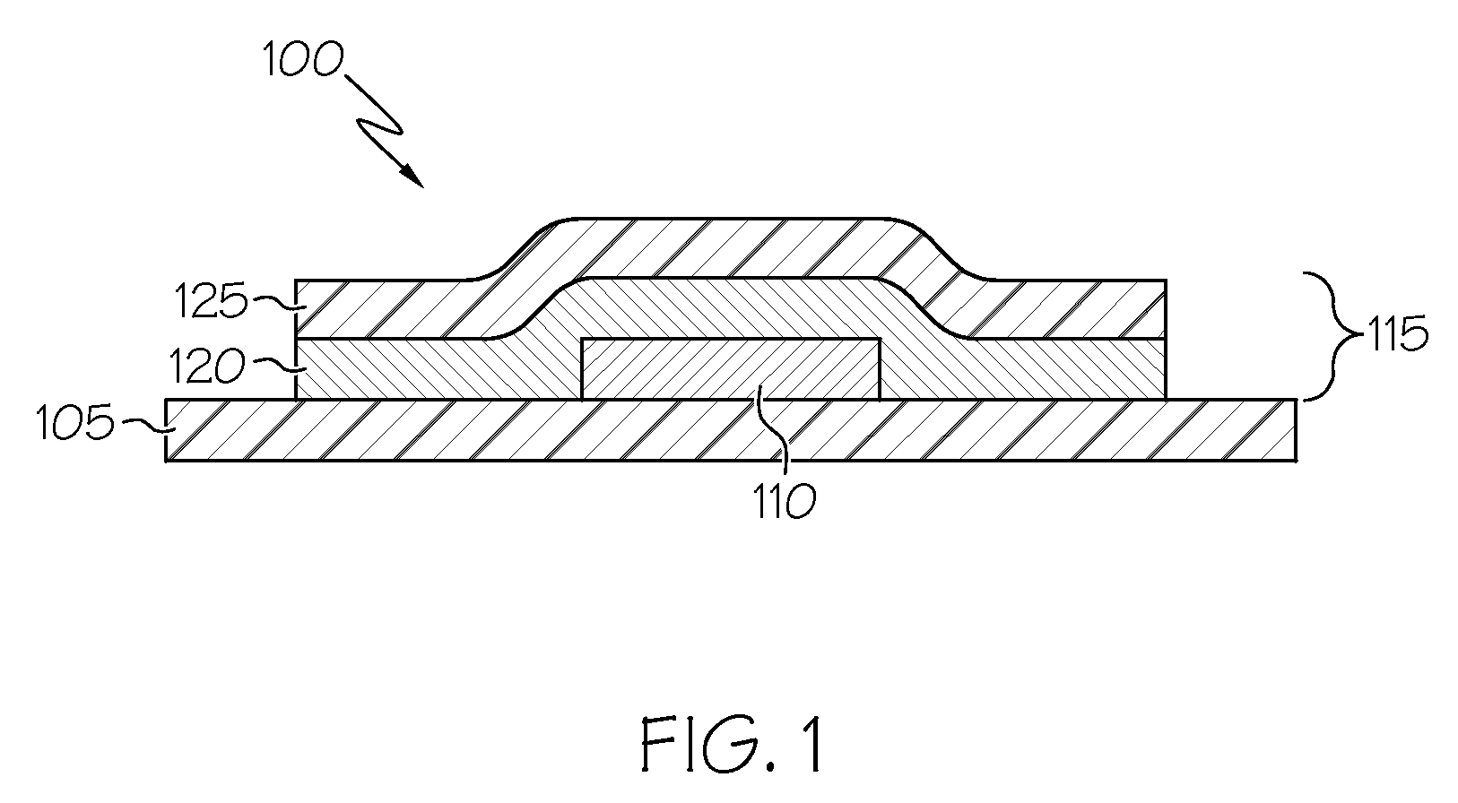
[0022] Another aspect of the invention is a method of reducing damage to a polymeric decoupling layer in a barrier stack. The method includes depositing the polymeric decoupling layer on a substrate; depositing a first inorganic layer on the decoupling layer under a first set of conditions wherein an ion and neutral energy arriving at the substrate is less than about 20 eV so that the first inorganic layer is not a barrier layer, wherein a temperature of the substrate is less than about 150°; and depositing a second inorganic layer on the first inorganic layer under a second set of conditions wherein an ion and neutral energy arriving at the substrate is greater than about 50 eV so that the second inorganic layer is a barrier layer.
[0024] Another aspect of the invention is a method of reducing damage to a polymeric decoupling layer in a barrier stack. The method includes depositing the polymeric decoupling layer on a substrate; placing a screen between a target and the substrate; plasma depositing a first inorganic layer on the decoupling layer under conditions so that the first inorganic layer is not a barrier layer; and plasma depositing a second inorganic layer on the first inorganic layer so that the second inorganic layer is a barrier layer

Problems solved by technology

Many devices are subject to degradation caused by permeation of environmental gases or liquids, such as oxygen and water vapor in the atmosphere or chemicals used in the processing of the electronic product.
We have found that some devices encapsulated with multilayer barrier stacks have been damaged by the plasma used in depositing the barrier and / or decoupling layers.
Device plasma damage has occurred when a substrate with a plasma sensitive device on it, such as an OLED, is encapsulated with a multi-layer barrier stack in which a plasma based and / or assisted process is used to deposit a barrier layer and / or decoupling layer on the OLED.
For example, device plasma damage has occurred when reactively sputtering a barrier layer of AlOx under conditions suitable for achieving barrier properties, sputtering a barrier layer of AlOx onto the top surface of a plasma sensitive device, and / or sputtering a barrier layer of AlOx on a vacuum deposited, acrylate based polymeric layer.
Device plasma damage associated with the use of plasma in the deposition of a barrier layer, a decoupling layer, or another layer on a device essentially has a negative impact on the electrical and / or luminescent characteristics of the encapsulated device.
For example, OLEDs made by some manufacturers show little to no device plasma damage, while OLEDs made by other manufacturers show significant device plasma damage under the same deposition conditions.
Device plasma damage results in higher voltage requirements to achieve the same level of luminescence (typically 0.2 to 0.5 V higher for an OLED), and / or lower luminescence.
Although not wishing to be bound by theory, device plasma damage that is observed when a decoupling layer employing plasma, a sputtered AlOx, or another layer employing plasma is formed (deposited) directly on an OLED or other sensitive device is believed to be due to an adverse interaction between the device and one or more components of the plasma, including ions, electrons, neutral species, UV radiation, and high thermal input.
On the other hand, it is known that, in some cases, plasma and / or radiation exposure degrades the functional properties of polymers (polymer plasma damage).
However, avoiding such processes is not always possible.

Method used


Image

  • Multilayer barrier stacks and methods of making multilayer barrier stacks
  • Multilayer barrier stacks and methods of making multilayer barrier stacks
  • Multilayer barrier stacks and methods of making multilayer barrier stacks

Examples


Embodiment Construction

[0051] In addition to the device plasma damage to the environmentally sensitive device caused by the plasma used in depositing the barrier and / or decoupling layers, in some circumstances, the deposition of an inorganic barrier layer using plasma based process or other high energy process can cause damage to the polymer layer on which it is deposited. For example, when a barrier layer is deposited using a sputtering or reactive sputtering process, damage to the polymeric decoupling layer can result. For purposes of this discussion, we will refer to the damage to the polymeric decoupling layer by any high energy process as “polymer plasma damage.” However, those having skill in the art will recognize that high energy processes include both plasma based processes and other high energy processes which do not involve the use of plasma. In the context of this discussion, by high energy processes, we mean processes in which ion and neutral energy arriving at the substrate is greater than a...


PUM

PropertyMeasurementUnit
Temperatureaaaaaaaaaa
Pressureaaaaaaaaaa
Pressureaaaaaaaaaa

Abstract

An improved barrier stack. The barrier stack is made by the process of depositing the polymeric decoupling layer on a substrate; depositing a first inorganic layer on the decoupling layer under a first set of conditions wherein an ion and neutral energy arriving at the substrate is less than about 20 eV so that the first inorganic layer is not a barrier layer, wherein a temperature of the substrate is less than about 150° C.; and depositing a second inorganic layer on the first inorganic layer under a second set of conditions wherein an ion and neutral energy arriving at the substrate is greater than about 50 eV so that the second inorganic layer is a barrier layer. Methods of reducing damage to a polymeric layer in a barrier stack are also described.

Description

CROSS REFERENCE TO RELATED APPLICATIONS [0001] This application is a continuation-in-part of application Ser. No. 11 / 439,474, filed May 23, 2006, entitled Method of Making an Encapsulated Plasma Sensitive Device, which is a continuation-in-part of application Ser. No. 11 / 112,880, filed Apr. 22, 2005, entitled Apparatus for Depositing a Multilayer Coating on Discrete Sheets, which is a continuation-in-part of application Ser. No. 10 / 412,133, filed Apr. 11, 2003, entitled Apparatus for Depositing a Multilayer Coating on Discrete Sheets, all of which are incorporated herein by reference.BACKGROUND OF THE INVENTION [0002] The present invention relates generally to multilayer barriers, and more particularly to multilayer barriers stacks having improved properties. [0003] Many devices are subject to degradation caused by permeation of environmental gases or liquids, such as oxygen and water vapor in the atmosphere or chemicals used in the processing of the electronic product. The devices ...

Claims


Application Information

Patent Timeline
IPC IPC(8): B32B9/04H01L21/469
CPCC23C14/024Y02E10/549H01L51/5237H01L51/448Y10T428/31678Y10T428/31663Y02P70/50H10K30/88H10K59/8731H10K50/8445
Inventor MORO, LORENZACHU, XI
Owner SAMSUNG DISPLAY CO LTD
Learn More