Organic Electroluminescent Element and Organic Electroluminescent Display

Active Publication Date: 2007-12-13
UDC IRELAND
View PDF10 Cites 20 Cited by
  • Summary
  • Abstract
  • Description
  • Claims
  • Application Information

AI Technical Summary

Benefits of technology

[0013] A general object of the invention, which was made in view of the problems above, is to provide an organic electro

Problems solved by technology

Therefore, there is a problem in that the luminance of the blue light emitted by the blue light-emitting layer decreases over time, so that the life of the organic EL element is shortened.
There is another problem in that the holes transferred into the electron-transport layer also recombine with electrons to cause the electron-transport layer to emit light in a color other than blue within a wavelength region close to the peak wavelength of blue, thereby deteriorating the blue chromaticity of the light emitted from the blue light-emitting layer.
However, if the method is applied to an organic EL element blue light-emitting layer, there is a problem in that the selection of the electron-transporting material constituting the electron-transport layer is greatly restricted.
However, because it is difficul

Method used


Image

  • Organic Electroluminescent Element and Organic Electroluminescent Display
  • Organic Electroluminescent Element and Organic Electroluminescent Display
  • Organic Electroluminescent Element and Organic Electroluminescent Display

Examples


Example

FIRST EMBODIMENT

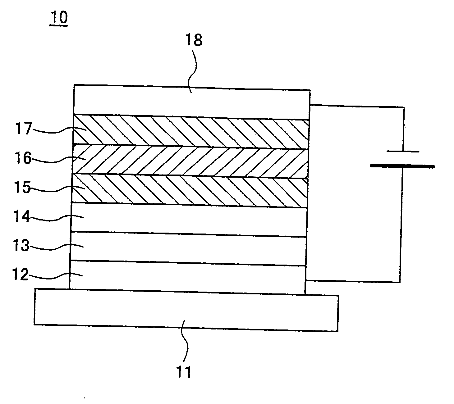
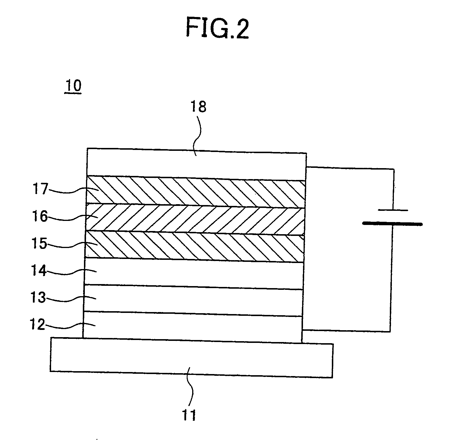
[0031]FIG. 2 is a cross-sectional view of an organic EL element according to the first embodiment of the invention. As shown in FIG. 2, the organic EL element 10 includes a glass substrate 11, and an anode 12, a hole-injecting layer 13, a hole-transport layer 14, a blue light-emitting layer 15, a hole-blocking layer 16, an electron-transport layer 17 containing an electron-transporting material and a light-emitting material having an emission spectrum peak wavelength of greater than 555 nm, and a cathode 18 provided on the glass substrate 11 in that order.

[0032] The organic EL element 10 has a film thickness of approximately 10 to 1,000 nm. A thickness of more than 1,000 nm leads to shielding of the light emitted in the blue light-emitting layer 15, while a thickness of less than 10 nm leads to insufficient luminance because the thickness of the blue light-emitting layer 15 itself is excessively small.

[0033] The anode 12 and the cathode 18 are electrodes for apply...

Example

FIRST EXAMPLE

[0057] An organic EL element of First Example was prepared in the following manner. On a glass substrate, an ITO electrode having a film thickness of 150 nm as an anode, a 2-TNATA layer as a hole-injecting layer having a film thickness of 140 nm and containing an acceptor F4-TCNQ (2,3,5,6-tetrafluoro-7,7,8,8-tetracyanoquinodimethane) in an amount of 0.1 vol %, an α-NPD layer as a hole-transport layer having a film thickness of 10 nm, a blue light-emitting layer consisting of a host material CBP which has a film thickness of 20 nm and which contains 1,3,6,8-tetra(4-biphenyl)pyrene in an amount of 10 vol %, a BAlq layer as a hole-blocking layer having a film thickness of 10 nm, an Alq (energy gap 2.73 eV) layer as an electron-transport layer which has a film thickness of 20 nm and which contains a light-emitting material chloro[2,3,7,8,12,13,17,18-octaethylporphrinato]iron (trivalent, manufactured by Kanto Kagaku Co. Inc.) in an amount of 1 vol % as an electron-transport...

Example

SECOND EXAMPLE

[0058] An organic EL element of Second Example is the same as that of First Example, except that a red light-emitting material, 5,10,15,20-tetraphenylporphine nickel (bivalent), was used in place of the light-emitting material used in the organic EL element of First Example. 5,10,15,20-tetraphenylporphine nickel (bivalent) was contained at a content of 1 vol % in Alq (energy gap 2.73 eV) . As shown in FIG. 4 below, because 5,10,15,20-tetraphenylporphine nickel (bivalent) has a peak wavelength of 655 nm, the energy gap of 5,10,15,20-tetraphenylporphine nickel (bivalent) is smaller than the energy gap of Alq (2.73 eV).

COMPARATIVE EXAMPLE

[0059] An organic EL element of Comparative Example is the same as that of First Example, except that the electron-transport layer is formed only with Alq (film thickness: 20 nm).

[0060] [Evaluation of Emission Spectrum, Chromaticity, and Luminance]

[0061] Relative distribution of the emission spectrum of each of the organic EL elements...


PUM

PropertyMeasurementUnit
Nanoscale particle sizeaaaaaaaaaa
Volumeaaaaaaaaaa
Wavelengthaaaaaaaaaa

Abstract

The invention relates to an organic EL element having a glass substrate and an anode, a hole-injecting layer, a hole-transport layer, a blue light-emitting layer, a hole-blocking layer, an electron-transport layer, and a cathode formed on the glass substrate sequentially in that order, wherein the electron-transport layer contains an electron-transporting material and a light-emitting material having emission-spectrum peak wavelength of longer than 555 nm, and the light-emitting material consumes the holes, thereby preventing degradation of the electron-transporting material, improving blue chromaticity, and elongating the life of the organic EL element.

Description

TECHNICAL FIELD [0001] The invention relates to an organic electroluminescent element and an organic electroluminescent display, and in particular, to an organic electroluminescent element and organic electroluminescent display having a blue light-emitting layer that emits blue light formed between an anode and a cathode. BACKGROUND ART [0002] Organic electroluminescent elements (hereinafter, organic electroluminescent elements will be referred to as “organic EL elements”), which are easier to reduce in size, lower in power consumption, and capable of surface light emission, and the use thereof in various display devices such as flat display is attracting attention since the applied voltage can be significantly reduced compared to liquid crystal elements. [0003] Such an organic EL element has a light-emitting layer and an electron-transport layer provided at the cathode side of the light-emitting layer, the electron-transport layer transporting electrons to the light-emitting layer....

Claims


Application Information

Patent Timeline
IPC IPC(8): H01J1/63C09K11/06H01L51/00H01L51/50H05B33/12H05B33/14
CPCC09K11/06Y10S428/917C09K2211/1029C09K2211/1088C09K2211/1092H01L51/0054H01L51/0059H01L51/006H01L51/0071H01L51/0072H01L51/0074H01L51/5048H01L51/5096H05B33/14C09K2211/1011H10K85/622H10K85/633H10K85/631H10K85/6576H10K85/657H10K85/6572H10K50/14H10K50/18
Inventor ITAI, YUICHIRO
Owner UDC IRELAND
Why Eureka
Try Eureka