Plasma processing apparatus and plasma processing method

Inactive Publication Date: 2007-12-13
TOKYO ELECTRON LTD
View PDF4 Cites 37 Cited by
  • Summary
  • Abstract
  • Description
  • Claims
  • Application Information

AI Technical Summary

Benefits of technology

[0040] The plasma processing apparatus according to the present invention comprises a selection passage implement configured to suppress passage of ions in plasma and preferentially allow hydrogen radicals in the plasma to pass therethrough. Consequently, for example, it is possible to remove the influence of ions onto a film formed on a wafer treated as the target substrate, and to perform curing of the film by hydrogen radicals without increasing the dielectric constant of the fi

Problems solved by technology

However, in the process of curing, a problem arises in th

Method used


Image

  • Plasma processing apparatus and plasma processing method
  • Plasma processing apparatus and plasma processing method
  • Plasma processing apparatus and plasma processing method

Examples


Embodiment Construction

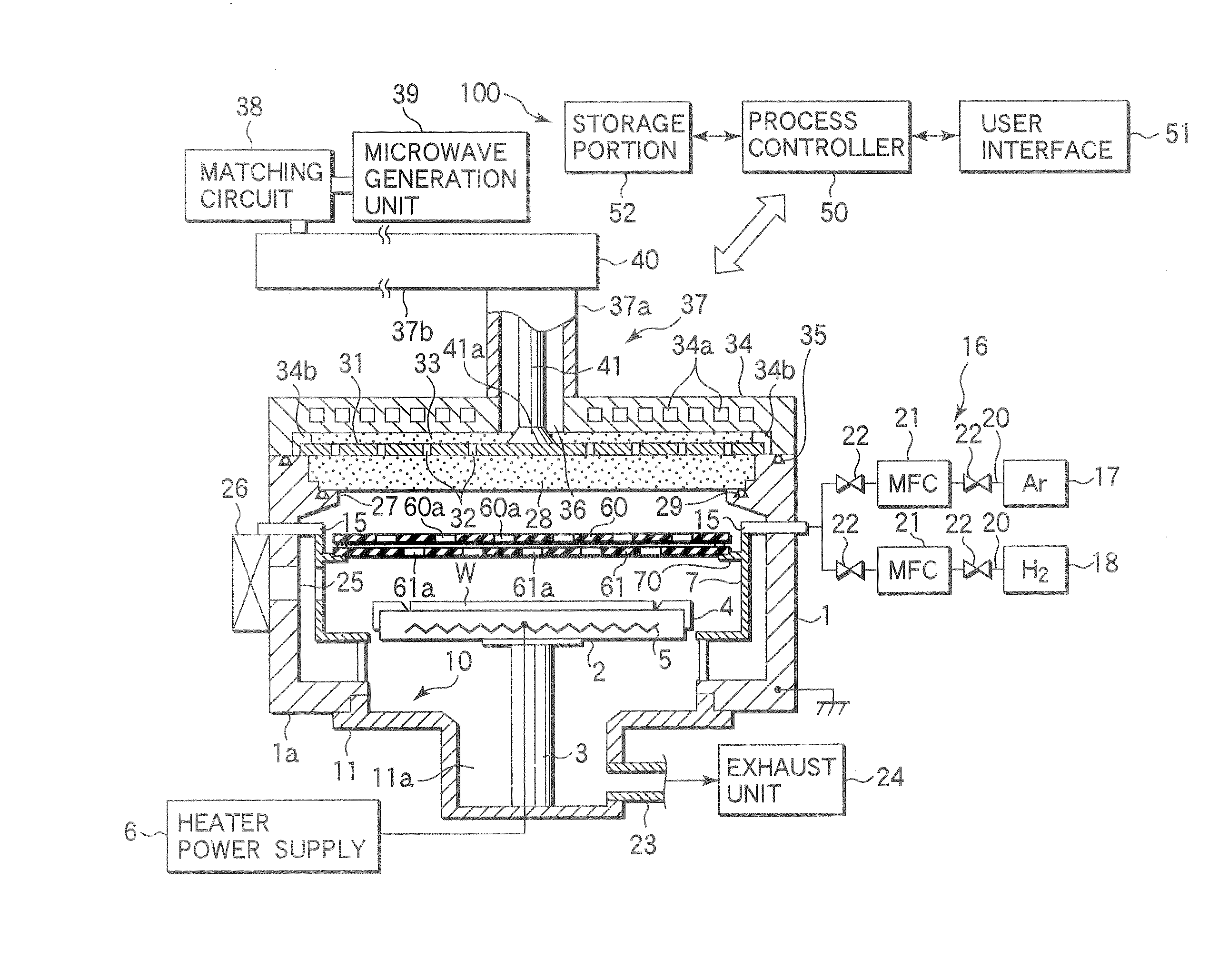
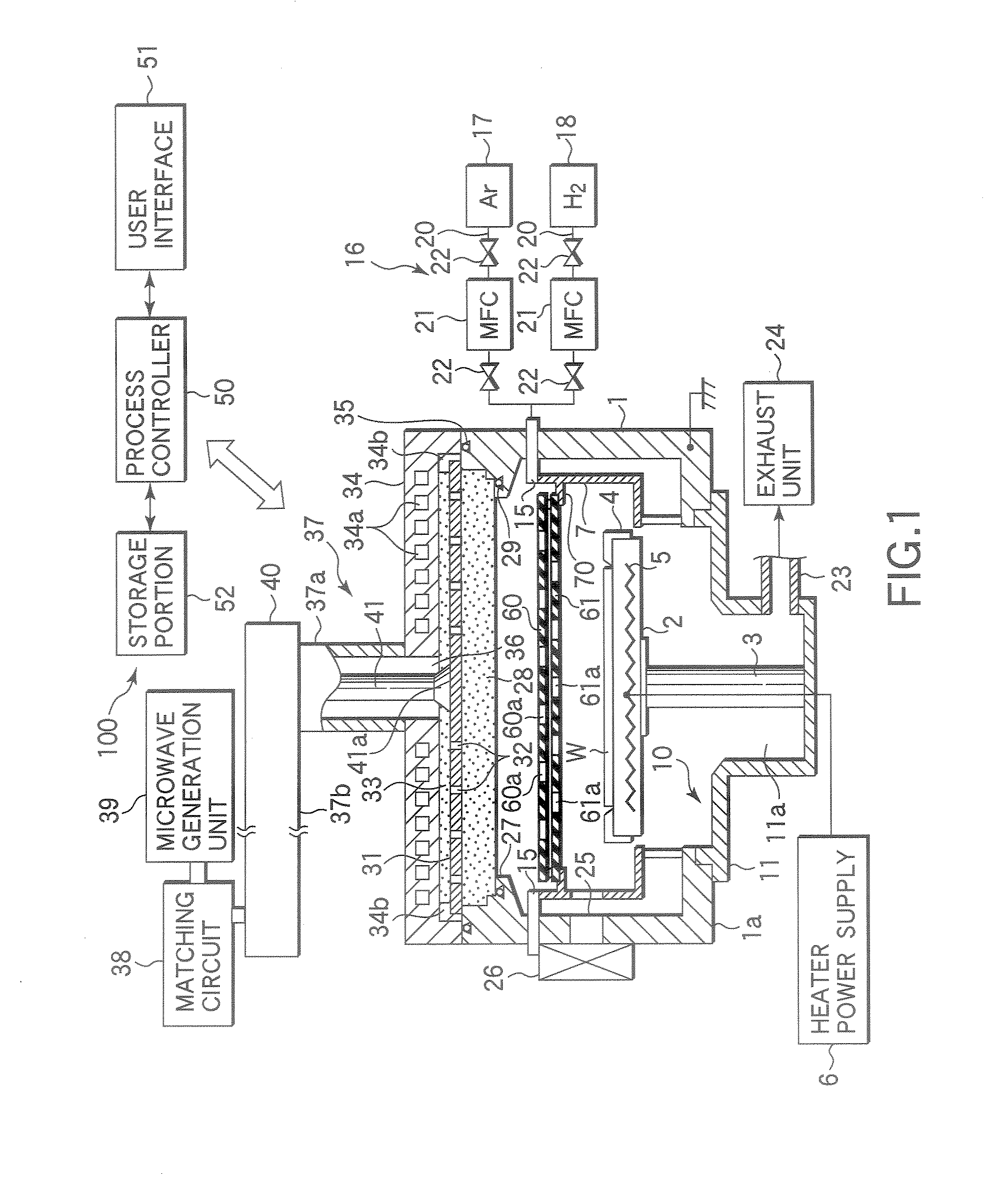
[0052] Preferable embodiments of the present invention will now be described with reference to the accompanying drawings. FIG. 1 is a sectional view schematically showing an example of a plasma processing apparatus according to an embodiment of the present invention. This plasma processing apparatus utilizes an RLSA (Radial Line Slot Antenna) plasma generation technique, in which microwaves are supplied from a planar antenna having a plurality of slots into a process chamber to generate plasma, so that microwave plasma is generated with a high density and a low electron temperature.

[0053] This plasma processing apparatus 100 can proceed with a plasma process at a low temperature of 500° C. or less and free from damage to the underlying film and so forth. Further this apparatus is good in plasma uniformity and thus can realize process uniformity comparable to those attained by plasma processing apparatuses of the ICP type and parallel-plate type. Accordingly, the plasma processing a...


PUM

PropertyMeasurementUnit
Lengthaaaaaaaaaa
Pressureaaaaaaaaaa
Electrical resistanceaaaaaaaaaa

Abstract

A plasma processing apparatus 100 includes an upper plate 60 and a lower plate 61 disposed above a susceptor 2. The upper plate 60 and lower plate 61 are made of a heat resistant and insulative material, such as quartz. The two plates are disposed in parallel with each other with a predetermined gap of, e.g., 5 mm interposed therebetween. The two plates have a plurality of through holes 60a and 61a formed therein and positionally shifted from each other. The two plates are disposed in an overlapped state such that the through holes 61a of the lower plate 61 are not aligned with the through holes 60a of the upper plate 60.

Description

TECHNICAL FIELD [0001] The present invention relates to a plasma processing apparatus for processing a target substrate, such as a semiconductor substrate, by use of plasma. BACKGROUND ART [0002] As regards high speed logic devices in recent years, inter-level insulating films tend to have a lower dielectric constant (progress in Low-k) to decrease the parasitic capacitance between interconnection lines. Accordingly, it has been studied to form Low-k films from porous materials having high porosity, for VLSI (very large scale integrated circuit) devices, and particularly for the 65-nm technical node generation or thereafter. In general, since porous Low-k films are poor in mechanical strength, film peeling may occur when planarization is performed by CMP after a Low-k film is formed and Cu is embedded. In light of this, the Low-k film needs to be processed in advance by a hardening process (curing) which is performed by, e.g., a heat process, UV process, or electron beam process. Th...

Claims


Application Information

Patent Timeline
IPC IPC(8): H05H1/24C23F1/00
CPCC23C16/5096C23C16/54C23C16/56H01J37/32422H01J37/3244H01L21/02126H01L21/31695H01L21/02216H01L21/02274H01L21/0234H01L21/3122H01L21/3127H01L21/31633H01L21/02203H01L21/3065
Inventor IDE, SHINJISASAKI, MASARU
Owner TOKYO ELECTRON LTD
Why Eureka
Try Eureka