
Method for Producing Nano-Scale Low-Dimensional Quantum Structure, and Method for Producing Integrated Circuit Using the Method for Producing the Structure

a low-dimensional quantum structure and integrated circuit technology, applied in the field of producing a nano-scale low-dimensional quantum structure and a method for producing an integrated circuit using the method for producing the structure, can solve the problems of not being able to precisely form the carbon nanotubes in the desired position, not being able to obtain a certain amount of carbon nanotubes, etc., and achieves the effect of high availability and effective us

Inactive Publication Date: 2007-12-13
JAPAN SCI & TECH CORP
View PDF7 Cites 18 Cited by
  • Summary
  • Abstract
  • Description
  • Claims
  • Application Information

AI Technical Summary

Benefits of technology

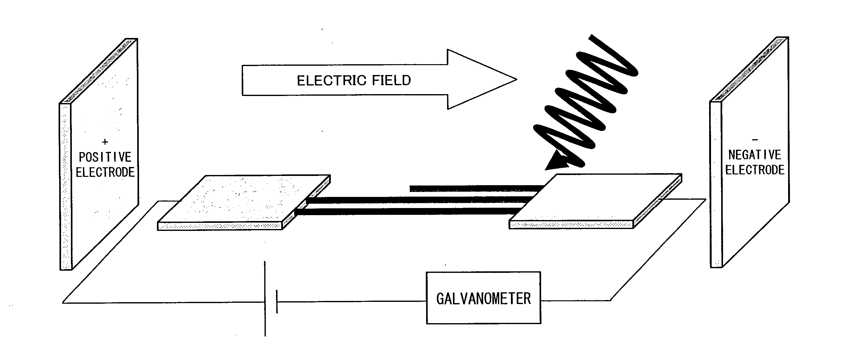
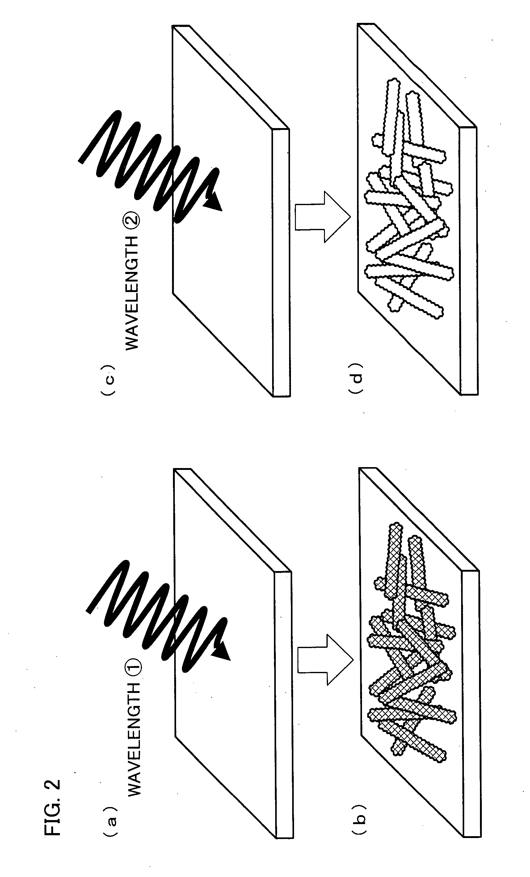
[0018] According to the arrangement, an electromagnetic wave is emitted, so that a catalyst which is positioned in an area (position) receiving the emitted electromagnetic wave and forms a nano-scale low-dimensional quantum structure thereon has higher temperature. The catalyst is in contact with gas (or liquid) containing elements constituting the nano-scale low-dimensional quantum structure. Thus, also gas (or liquid) containing elements constituting a nano-scale low-dimensional quantum structure around the catalyst has higher temperature, which results in thermal decomposition, so that a nano-scale low-dimensional quantum structure is formed on the catalyst. Thus, by controlling an electromagnetic wave, it is possible to form a nano-scale low-dimensional quantum structure in a target area.
[0019] Further, by controlling the electromagnetic wave for local emission, it is possible to locally form a nano-scale low-dimensional quantum structure in a target position on the catalyst. By utilizing this arrangement, it is possible to sequentially form nano-scale low-dimensional quantum structures in different positions. According to the arrangement, such formation can be carried out only by sequentially changing areas to which the electromagnetic wave is emitted, so that the arrangement is optimal for manufacturing application. For example, in case where the nano-scale low-dimensional quantum structure is a single-walled nanotube, the structure is highly available particularly in an integrated circuit. That is, in the integrated circuit, it is necessary to allow an intended number of single-walled carbon nanotubes having different properties (chiralities) to cross-link and grow between electrodes so as to be positioned in local areas different from each other, so that the aforementioned method can be effectively used.

Problems solved by technology

According to the ark discharge method, it is possible to obtain high quality carbon nanotubes having less defects, but it is difficult to obtain a certain amount of carbon nanotubes.
However, none of the aforementioned methods allows formation of the carbon nanotubes in a target area.
However, it is impossible to form the carbon nanotubes exactly in a desired position, particularly in a local position.
Further, a conventional method for forming carbon nanotubes is not suitable for sequentially forming carbon nanotubes in desired positions on the catalyst.
Such repetition is unfavorable in view of efficiency.
The second reason is such that: In case of the CCVD carried out by electroheating, it is possible to sequentially form carbon nanotubes in target positions, but it is necessary to pattern a circuit for the electrification in advance, and it is impossible to locally heat a particular target area.
Further, in the present circumstances, there is no method for selectively producing carbon nanotubes having a specific state density.
Also, there is no method for allowing an intended number of carbon nanotubes to cross-link.

Method used


Image

  • Method for Producing Nano-Scale Low-Dimensional Quantum Structure, and Method for Producing Integrated Circuit Using the Method for Producing the Structure
  • Method for Producing Nano-Scale Low-Dimensional Quantum Structure, and Method for Producing Integrated Circuit Using the Method for Producing the Structure
  • Method for Producing Nano-Scale Low-Dimensional Quantum Structure, and Method for Producing Integrated Circuit Using the Method for Producing the Structure

Examples


embodiment

[0045] With reference to FIGS. 1 to 6, the following describes one embodiment of the present invention. Note that, the present invention is not limited to the embodiment.

[0046] Note that, in the present embodiment, single-walled carbon nanotubes are produced as a nano-scale low dimensional quantum structure. However, a product which can be produced in accordance with the present invention is not limited to the single-walled carbon nanotubes. Examples of the product include multi-walled carbon nanotubes, carbon nanohorn, boron nitride, carbon nanofiber, carbon nanocoil, fullerene, and the like.

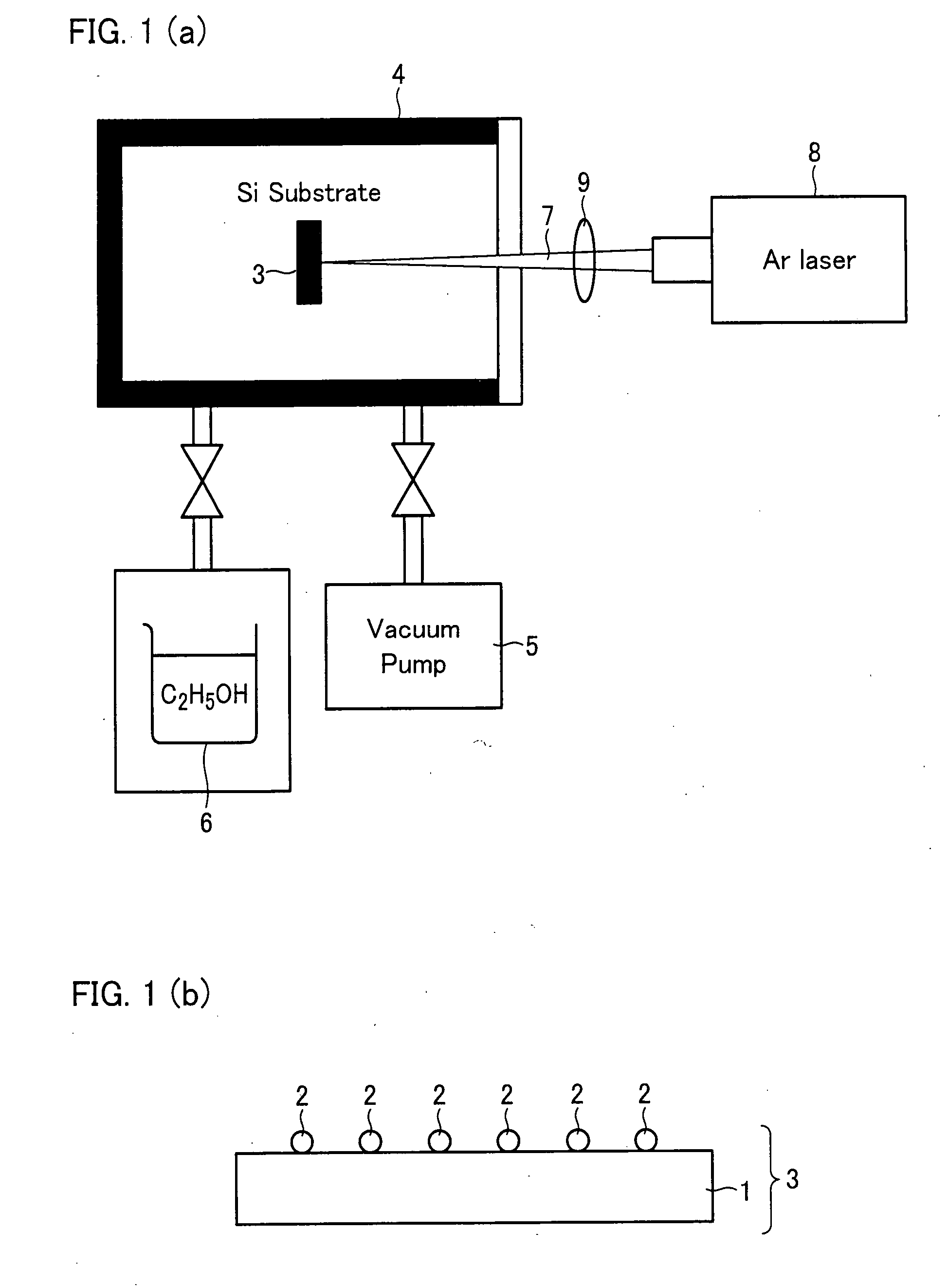
[0047] The production method of the single-walled carbon nanotubes is as follows. First, as illustrated in FIG. 1(b), a catalyst 2 for forming single-walled carbon nanotubes are applied to a substrate 1.

[0048] Any material may be used for the substrate 1 as long as the material can resist high temperature caused by emission of an electromagnetic wave. Examples of the material include silicon...

example

[0079] Example of the present invention is detailed as follows with reference to Experiments 1 to 6. However, the present invention is not limited to the Example. Note that, all the experiments were carried out at room temperature.

experiment 1

[Experiment 1] Formation of Substrate

[0080] A catalyst containing iron (Fe), molybdenum (Mo), and aluminum oxide (Al2O3) was applied to an Si substrate. Here, a catalyst of iron (Fe), a catalyst of molybdenum (Mo), and a catalyst of aluminum oxide (Al2O3) were mixed with one another by using methanol, and the mixture was dropped onto the substrate, thereby applying the mixed catalysts to the substrate.

[0081] Note that, in the present example, the catalysts were mixed as follows by using the following chemicals.

Chemical A: Iron (III) nitrate nonahydrate 98% (iron-containing solid)

Fe(No3)3.9H2O (product of Aldrich Company)

Chemical B: Bis(acetylacetonato)-dioxomolybdenum (IV)

(molybdenum-containing solid)

(C5H8O2)2MoO2 (product of Aldrich Company)

Chemical C: Aluminum oxide (aluminum oxide solid)

“Fumed Alumina” Al2O3 (product of Degussa Company)

[0082] First, 40 mg of the chemical A, 3 mg of the chemical B, and 30 mg of the chemical C were placed in a beaker, and 30 ml of me...


PUM


Abstract

A method of an embodiment of the present of the present application is for producing a nano-scale low dimensional quantum structure. The method includes: bringing a catalyst on a substrate into contact with vaporized carbon source, and emitting an electromagnetic wave to the catalyst so as to form single-walled carbon nano-tubes on the catalyst. As a result, it is possible to form the nano-scale low-dimensional quantum structure on a target area.

Description

TECHNICAL FIELD [0001] The present invention relates to a method for producing a nano-scale low-dimensional quantum structure and a method for producing an integrated circuit using the method for producing the structure. Particularly, the present invention relates to a method for producing carbon nanotubes and a method for producing an integrated circuit using the method for producing the carbon nanotubes. BACKGROUND ART [0002] The development of high-tech materials and new materials has a significant importance as it forms the basis of industry and science and technology in a wide variety of fields such as electronics, information communications, environment energy, biotechnology, medicine, and bioscience. [0003] In recent years, the development of nano-scale substances has drawn many interests since they possess totally novel properties and functions not found in bulk substances. [0004] Carbon nanotubes are an example of such a nano-scale substance. It is known that the carbon nan...

Claims


Application Information

Patent Timeline
IPC IPC(8): H01L21/71C25B5/00
CPCB82Y10/00B82Y30/00H01L51/0048C01B31/0233B82Y40/00C01B32/162H10K85/221
Inventor MAEHASHI, KENZOFUJIWARA, YASUYUKIINOUE, KOICHIMATSUMOTO, KAZUHIKOOHNO, YASUHIDE
Owner JAPAN SCI & TECH CORP
Learn More