
Electronic device, dielectric ceramic composition and the production method

a technology of dielectric ceramic and dielectric device, which is applied in the direction of fixed capacitors, electrical apparatus, domestic applications, etc., can solve the problems of low specific permittivity of dielectric ceramic composition described in the article, unable to respond to downsizing and obtaining of a larger capacity, and liable to have little flexibility to obtain characteristics according to application, so as to achieve high specific permittivity

Inactive Publication Date: 2007-12-13
TDK CORPARATION
View PDF9 Cites 21 Cited by
  • Summary
  • Abstract
  • Description
  • Claims
  • Application Information

AI Technical Summary

Benefits of technology

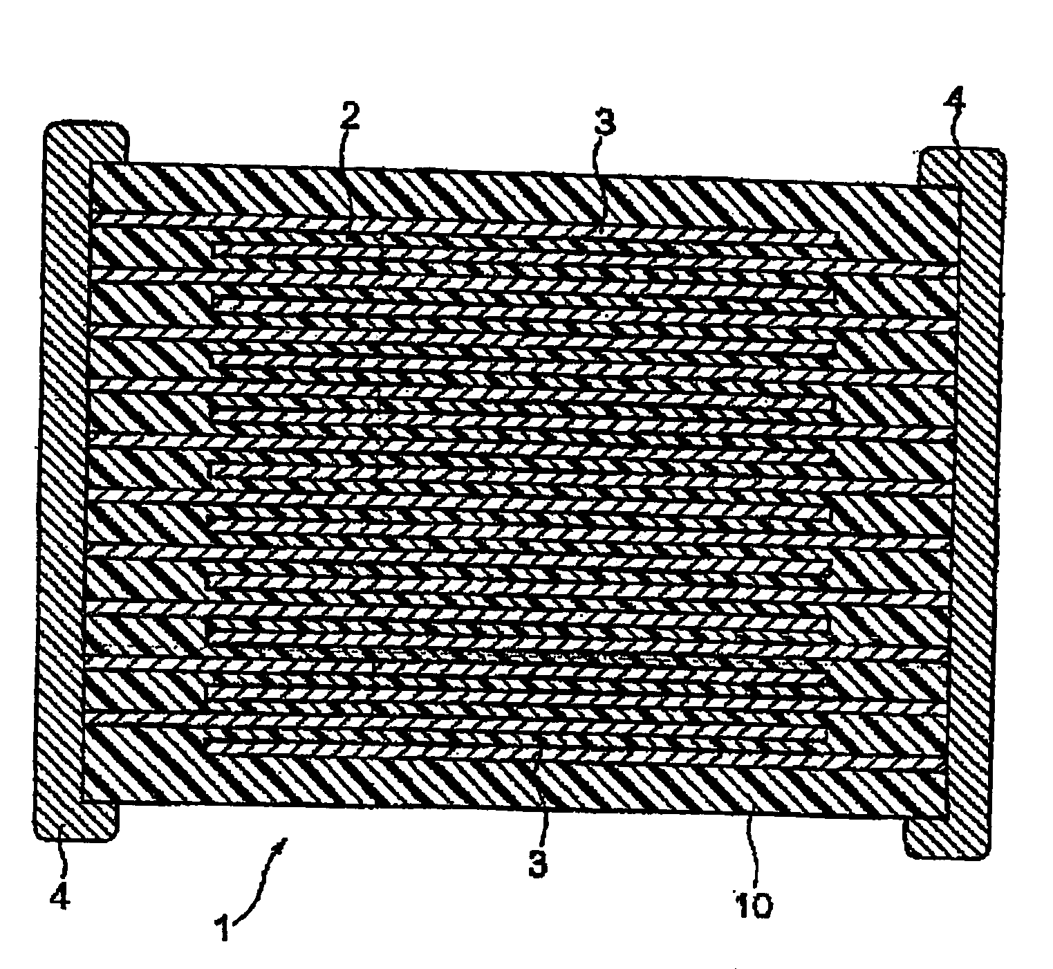
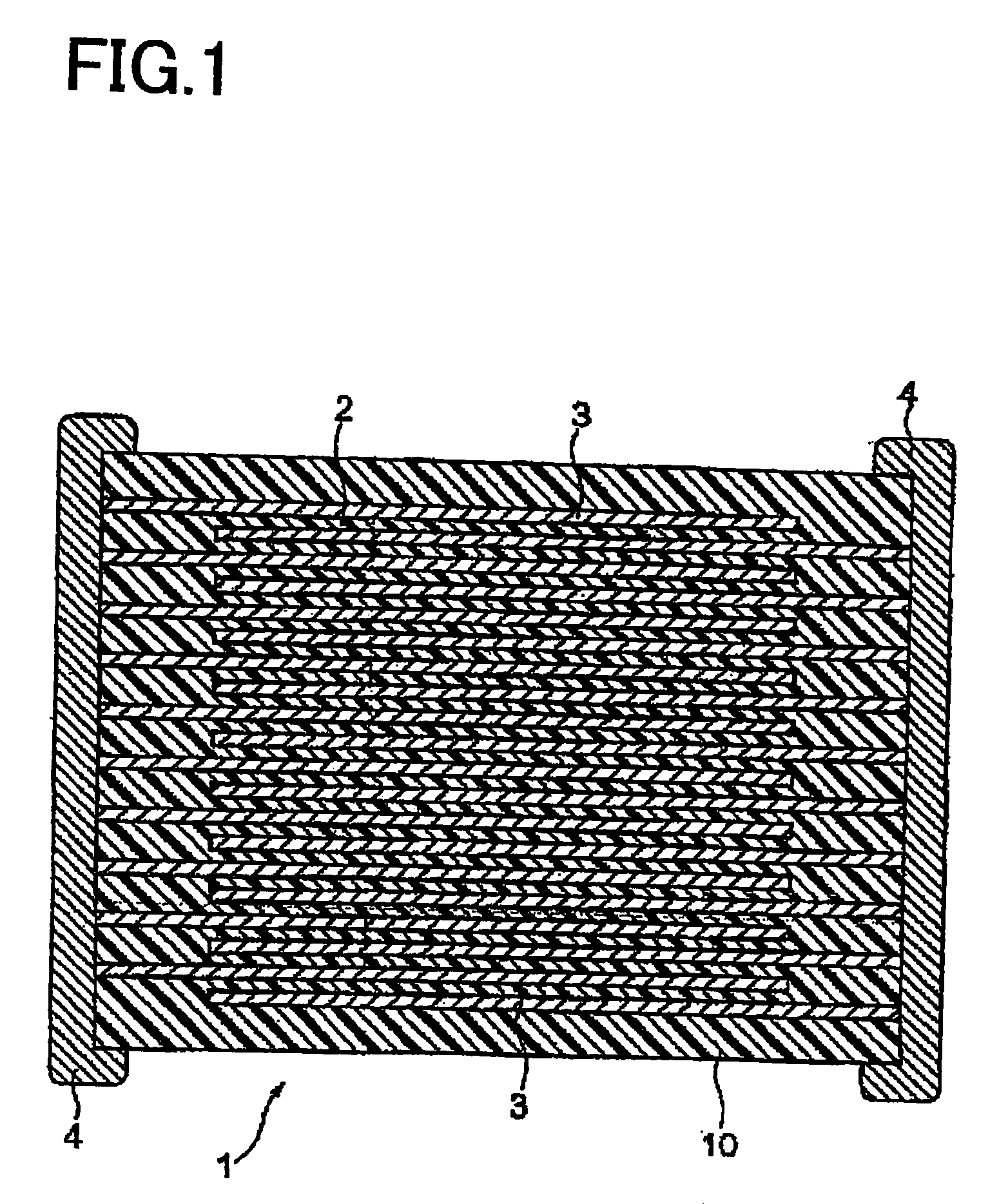
[0011]An object of the present invention is to provide a dielectric ceramic composition, capable of making dielectric layers thin, of exhibiting high specific permittivity and a preferable temperature characteristic of capacitance, and of improving reliability even when the main component of the dielectric ceramic composition varies, and the production method thereof. Another object of the present invention is to provide an electronic device, such as a multilayer ceramic capacitor, having a dielectric layer composed of a dielectric ceramic composition as such.
[0012]The present inventors have found that it is possible to obtain dielectric ceramic composition having a high specific permittivity and preferable temperature characteristic of capacitance as well as preferable other characteristics by using a specific method for adding oxides of rare earth element added as subcomponents even when making the dielectric layers thinner and selecting a main component from a variety of compounds having a perovskite-type crystal structure. Also, the present inventors have found that the above effects could be furthermore enhanced by dividing the above rare earth elements to two groups based on a value of effective ionic radius for coordination number 9, by using a specific method for adding oxides of elements selected from one or both of the two groups, and by setting a ratio of number of moles of elements belonging to one group and number of moles of elements belonging to the other group in the two groups to be in a specific range in the finally obtained dielectric ceramic composition, and completed the present invention.

Problems solved by technology

Therefore, in the related art, it has been necessary to use expensive precious metals, such as platinum and palladium, as the material composing the internal electrode layer.
However, when dielectric layers are made thin, an electric field imposed on the dielectric layers becomes stronger at the time of applying a direct current voltage, consequently, there has been a disadvantage that a change of the specific permittivity with time, that is, a change of the capacity with time becomes remarkably large.
However, the dielectric ceramic composition described in the article has too low specific permittivity to respond to downsizing and obtaining of a larger capacity.
However, in the Japanese Unexamined Patent Publication No. 2005-29423, the main component of a dielectric ceramic composition is limited to barium titanate, it is liable to have little flexibility to obtain characteristics according to application.

Method used


Image

  • Electronic device, dielectric ceramic composition and the production method
  • Electronic device, dielectric ceramic composition and the production method

Examples


example 1

[0158]First, BaTiO3 and CaTiO3 powders having an average particle diameter of 0.30 μm as the main component material and Y2O3 powder as the fourth subcomponent material to be reacted in advance (pre-added material) were prepared. Next, the prepared main component powders and a part of Y2O3 powder were weighed to obtain respective amounts shown in Table 1, wet mixed / pulverized by a ball mill to obtain slurry. After drying the slurry, calcination and pulverizing were performed, so that a post-reaction material was obtained. Note that the calcination condition was the temperature raising rate of 200° C. / hour, the holding temperature of 500° C., the temperature holding time of two hours and an atmosphere in the air. Namely, in the sample 1, only BaTiO3 powder was used as the main component material. An amount of Y2O3 to be reacted in advance was 0.1 mole in terms of Y atom (0.05 mole in terms of Y2O3) with respect to 100 moles of the main component (note that an amount of Y2O3 will be i...

example 2

[0184]As with sample 1, only BaTiO3 powder was used as the main component material, and Y2O3 (the fourth (a) subcomponent) was used as a material to be reacted in advance. Also, except for changing an amount of Y2O3 (the fourth (a) subcomponent) reacted in advance with the main component material to a value shown in Table 2 in terms of Y atom and amounts of Y2O3 (the fourth (a) subcomponent) and Gd2O3 (the fourth (b) subcomponent) added to the post-reaction material to values shown in Table 2 in terms of Y atom and Gd atom, each capacitor sample was obtained as with sample 1. The obtained respective samples were evaluated in the same way as in the example 1. The results are shown in Table 2.

[0185]Note that the ratio M2 / M1 between number of moles M1 of R1 of the fourth (a) subcomponent (pre-adding 0.05 mole and post-added 0.55 mole=0.6 mole) and number of moles M2 of R2 of the fourth (b) subcomponent (0.05 mole) in the finally-obtained dielectric ceramic composition was 0.08 in the e...

example 3

[0188]As with sample 1, only BaTiO3 powder was used as the main component material, and Yb2O3 (the fourth (a) subcomponent) was used instead of Y2O3 (the fourth (a) subcomponent) as a material to be reacted in advance. Also, except for changing an amount of Yb2O3 (the fourth (a) subcomponent) reacted in advance with the main component material and amounts of Y2O3 (the fourth (a) subcomponent) and Gd2O3 (the fourth (b) subcomponent) added to the post-reaction material to values shown in Table 3 in terms of R1 and R2 respectively, each capacitor sample was obtained as with the example 1. The obtained respective samples were evaluated in the same way as in the example 1. The results are shown in Table 3.

[0189]Note that the ratio M2 / M1 between number of moles M1 of R1 of the fourth (a) subcomponent and number of moles M2 of R2 of the fourth (b) subcomponent in the finally-obtained dielectric ceramic composition was 0.08 in the example 3.

TABLE 3SubcomponentTemper-MainPre-addingPost-addin...


PUM

PropertyMeasurementUnit
Molar densityaaaaaaaaaa
Substance countaaaaaaaaaa

Abstract

A production method of a dielectric ceramic composition comprising a main component including a compound having a perovskite-type crystal structure expressed by a composition formula (Ba1-xCax) (Ti1-yZry)O3 (note that 0≦x≦0.2, 0≦y≦0.2), and a fourth subcomponent including an oxide of R (note that R is at least one selected from Y, La, Ce, Pr, Nd, Pm, Sm, Eu, Gd, Tb, Dy, Ho, Er, Tm, Yb and Lu); comprising steps of obtaining a post-reaction material by bringing a material of the main component to react in advance with a part of a material of the fourth subcomponent to be included in the dielectric ceramic composition, and adding rest of material of the fourth subcomponent to be included in the dielectric ceramic composition into the post-reaction material. According to the present invention, both of a dielectric ceramic composition capable of improving the specific permittivity and a temperature characteristic of capacitance can be preferable, and the production method can be provided.

Description

BACKGROUND OF THE INVENTION[0001]1. Field of the Invention[0002]The present invention relates to a dielectric ceramic composition used as a dielectric layer of an electronic device, such as a multilayer ceramic capacitor, a production method thereof and an electronic device comprised of the dielectric ceramic composition as a dielectric layer.[0003]2. Description of the Related Art[0004]A multilayer ceramic capacitor as an example of electronic devices is produced, for example, by printing internal electrodes in a predetermined pattern on a ceramic green sheet formed by a predetermined dielectric ceramic composition, alternately stacking the results to form as one body, and co-firing a thus obtained green chip. Since internal electrode layers of the multilayer ceramic capacitor are formed to be one body with ceramic dielectric by firing, materials not reacting with the ceramic dielectric have to be selected. Therefore, in the related art, it has been necessary to use expensive preci...

Claims


Application Information

Patent Timeline
IPC IPC(8): C04B35/468C04B35/00B28B3/00
CPCB82Y30/00H01G4/30C04B35/49C04B35/6263C04B35/6264C04B35/62685C04B35/638C04B2235/3203C04B2235/3206C04B2235/3208C04B2235/3213C04B2235/3215C04B2235/3224C04B2235/3225C04B2235/3227C04B2235/3229C04B2235/3236C04B2235/3239C04B2235/3241C04B2235/3248C04B2235/3256C04B2235/3258C04B2235/3262C04B2235/3409C04B2235/3418C04B2235/3436C04B2235/3445C04B2235/3454C04B2235/441C04B2235/449C04B2235/5445C04B2235/5454C04B2235/652C04B2235/6562C04B2235/6565C04B2235/6567C04B2235/6582C04B2235/6584C04B2235/6588C04B2235/663C04B2235/768C04B2235/785H01G4/1227C04B35/4682H01B3/10
Inventor YANAGIDA, MIYUKISATO, AKIRA
Owner TDK CORPARATION
Learn More