Solar Cell Module and Photovoltaic Power Generator Using This

a solar cell module and solar cell technology, applied in the field of solar cell modules and photovoltaic power generators, can solve the problems of high production cost of substrates, difficult improvement of conversion efficiency, multicrystalline silicon solar cells, etc., and achieve the effect of reducing the ratio of outer peripheral regions, improving power generation efficiency (amount of power generation/area of solar cell modules), and improving design quality

Inactive Publication Date: 2007-12-27
KYOCERA CORP
View PDF15 Cites 182 Cited by
  • Summary
  • Abstract
  • Description
  • Claims
  • Application Information

AI Technical Summary

Benefits of technology

[0070] This structure makes it possible to reduce the ratio of the outer peripheral region of the solar cell module that has a different color from that of the solar cell elements, and thereby to render a dark tone of the color of the surfaces of the solar cell elements, which is something between blue and dark blue near black, to the solar cell module. As a result, the design quality of the solar cell module can be further improved, as well as the power generation efficiency (amount of power generation / area of solar cell module) of the solar cell module can be improved owing to the high proportion of the solar cell elements.
[0071] The spacing between the plurality of solar cell elements is preferably not less than 70% and not more than 143% of the widths of the wiring members. This allows the spacings between the solar cell elements and the widths of the wiring members to be generally equal, which makes a plurality of lines in the same direction appear to be penetrating the solar cell module, as an overall impression of the solar cell module. Thus, the design quality of the solar cell module can be further improved.
[0072] By designing all the widths of the plurality of wiring members visible from the light receiving surface side to be generally identical, it is possible to prevent the wiring members from appearing to be uneven, thereby further improving the design quality of the solar cell module.
[0073] In addition, by determining the widths of the wiring members to be not less than 0.8 mm and not more than 2.0 mm, the wiring members can be prevented from being noticeable.

Problems solved by technology

An advantage of monocrystalline silicon solar cells is that improvement of the conversion efficiency is easy because of the high quality of the substrates, while a disadvantage thereof is high production cost of the substrates.
On the other hand, multicrystalline silicon solar cells have a drawback that improvement of the conversion efficiency is difficult due to inferior quality of the substrates, and an advantage that they can be produced at low cost.
However, a problem is that, in particular, when finger electrodes are thinned to decrease the electrode area, the resistance within the electrode increases, resulting in loss.
However, in reality, there is a limit to the thickness of electrodes when electrodes are formed by screen printing, and the desired thickness can only be obtained through a process including a plural times of printing, and by using expensive equipment, namely, that for sputtering or vapor deposition.
This leads to the problem of increase in solar cell production cost.
This is because even the silicon solar cell element that is dominant in the market produces only a low voltage on the order of 600 V when used as a single element and is not practical, the cells therefore need to be series connected to increase the voltage.
This difference in color is one factor to deteriorate the design quality of the solar cell module.
However, in such a case, the following problems arise: the cost for the glass material increases; large scale equipment is necessary for forming an antireflective film on the surface of the glass; and the production cost increases because the number of processes increases.
In addition, when irregularities are formed on the surface of the glass, dirt and dust tend to adhere to the solar cell module that is set outside due to exposure to the elements, which intercept the sunlight before it enters the solar cell module, causing the solar cell module to have degraded output characteristics.
Similarly, in the case of a solar cell module provided with an anti-glare film inside thereof, although the problem of light pollution can be prevented, additional materials are required and the production cost increases.
In addition, the effect to enhance light diffusion / reflection obtained by using white color for the filler member 10 or a back surface protective member 11 located on the back surface side of the solar cell elements of a solar cell module cannot be expected, which hinders improvement of the properties of the solar cell module.
However, since covering the surfaces of the wiring members 8 and connecting members 6 causes the problem of increase in material cost and the number of steps, and large scale equipment is required for forming a film on all of the solar cell elements connected through the wiring members 8, the production cost increases.
However, since this requires an additional step of coloring the translucent panel 9 and positioning between the translucent panel 9 that has predetermined, preliminarily colored regions and the solar cell elements connected through wiring members 8, the process becomes complicated.
In addition, the effect to enhance light diffusion / reflection obtained by using white color for the filler member 10 or the back surface material 11 located on the back surface side of the solar cell elements cannot be expected, hindering improvement of the properties of the solar cell module.
As described so far, despite the highmarket demand, it has been difficult to realize the production of a solar cell module with high efficiency and high design quality at low cost.

Method used


Image

  • Solar Cell Module and Photovoltaic Power Generator Using This
  • Solar Cell Module and Photovoltaic Power Generator Using This
  • Solar Cell Module and Photovoltaic Power Generator Using This

Examples


example

[0285] Hereinafter, the results of experiments conducted on solar cell elements fabricated according to the foregoing embodiments will be shown.

[0286] As the substrate, a flat plate p-type multicrystalline silicon substrate of 150 mm×150 mm in size fabricated by a casing method having a specific resistivity of 2Ω·cm was used.

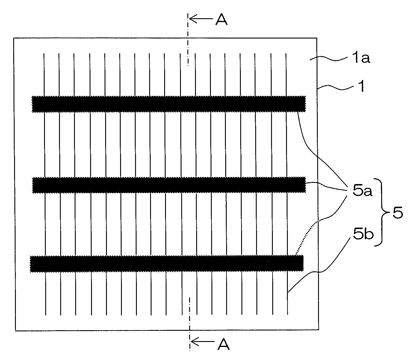
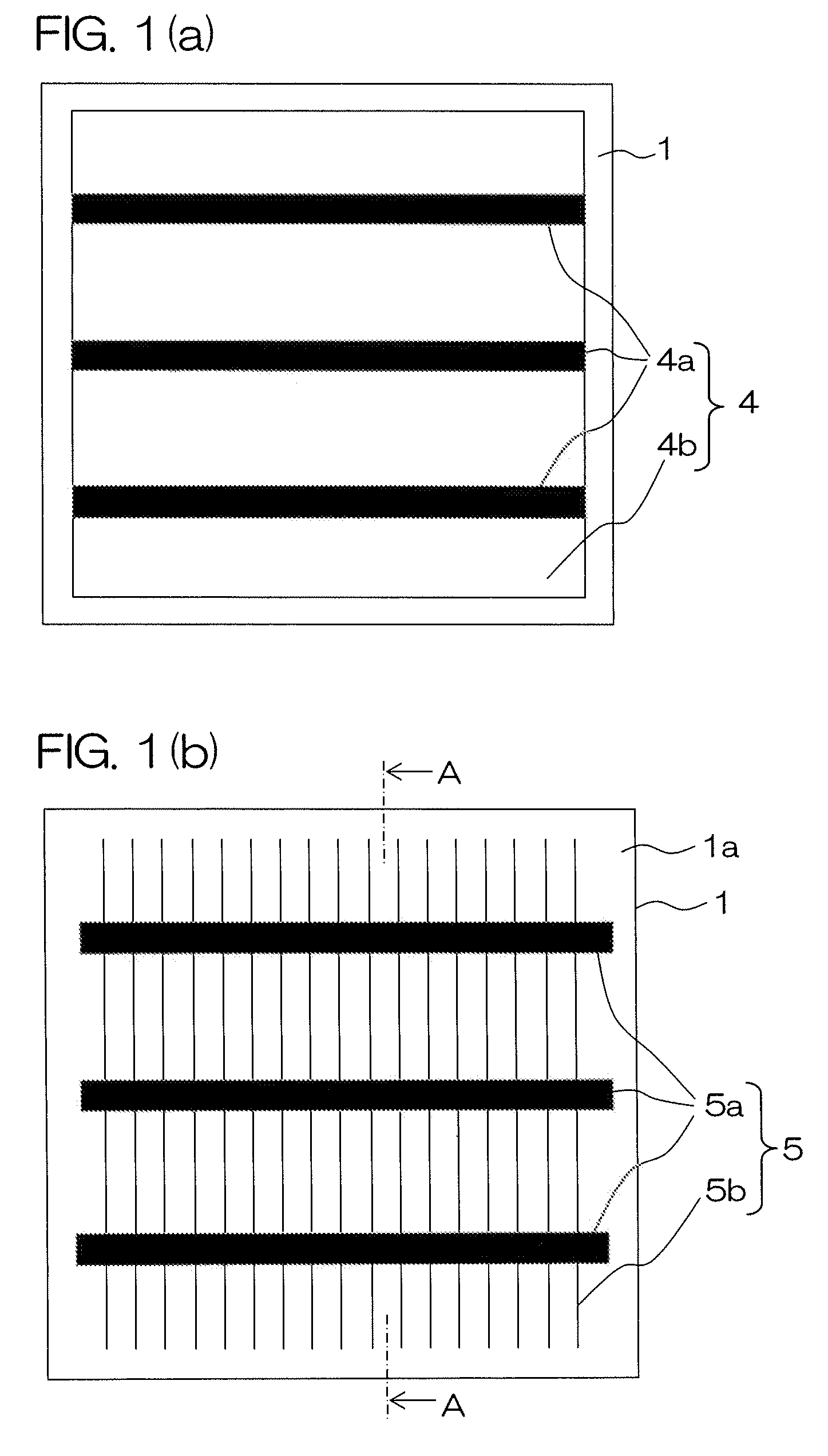
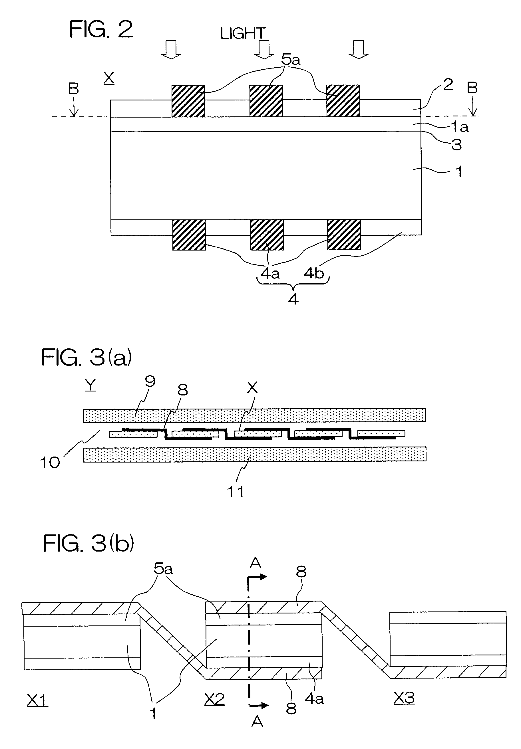
[0287] A paste including silver as a main component was printed and baked to form a surface electrode. The pattern for the surface electrode as a whole was formed by disposing three lines including one vertical line at the center of the substrate, and two lines axisymmetrically thereto. The bus bar electrodes 5a were made to have a length of 148.8 mm.

[0288] The widths of the bus bar electrodes 5a were varied to eight different values as 0.6, 0.8, 1.0, 1.2, 1.4, 1.6, 1.8, 2.0 mm.

[0289] The distance between the center lines of the bus bar electrodes 5a was 49.3 mm, the length of finger electrodes from one end to the other end of the substrate (including the wi...

example 2

[0297] The relationship between the configuration of the surface electrode and the characteristic was investigated on a bulk-type crystalline silicon solar cell as the solar cell element fabricated according to the foregoing embodiment.

[0298] As the substrate, a flat plate p-type multicrystalline silicon substrate of 150 mm×155 mm in size fabricated by a casting method was used, and solar cell elements with the structure shown in FIG. 4(a) were formed.

[0299] A paste including silver as a main component was printed and baked to form the surface electrode according to the solar cell element of the present invention.

[0300] The pattern for the surface electrode as a whole was formed, such that when the substrate was oriented to have a length of 150 mm in the vertical direction and 155 mm in the horizontal direction in FIG. 4(a), the length of bus bars 5a disposed axisymmetrically to the vertical center line of the substrate was 147.5 mm, the width of the bus bar electrodes 5a is 2 mm...

example 3

[0320] Subsequently, the relationship between the roughness of the contact surface between the surface electrode and the semiconductor substrate and the solar cell element characteristics was examined.

[0321] A flat plate p-type multicrystalline silicon substrate of 150 mm×150 mm in size fabricated by casting was used as the substrate to form a solar cell element with the structure shown in FIG. 1(a).

[0322] A paste including silver as a main component was printed and baked to form the surface electrode according to the present invention. The pattern for the surface electrode as a whole was formed according to the following dimensions. The length of two bus bar electrodes 5a disposed axisymmetrically to the vertical center line of the substrate was 148.8 mm. The width of the bus bar electrodes 5a was 2 mm, the distance between the center lines of two bus bar electrodes 5a was 75 mm, the length of finger electrodes 5b from one end to the other end of the substrate (including the widt...


PUM


Abstract

A surface electrode (5) is installed on the light receiving surface of a solar cell element, the surface electrode (5) comprises three bus bar electrodes (5a) for extracting light-produced at the solar cell element to the outside and collecting finger electrodes (5b) connected to these bus bar electrodes (5a), and the bus bar electrodes (5a) are not less than 0.5 mm and not more than 2 mm in width and the finger electrodes (5b) are not less than 0.05 mm and not more than 0.1 mm in width. A high-efficient solar cell module can be obtained with substantially lowered resistance by increasing the number of bus bar electrode (5a) and thereby decreasing the lengths of the finger electrodes (5b).

Description

TECHNICAL FIELD [0001] The present invention relates to a solar cell module using solar cell elements including a surface electrode on the light receiving surface thereof and a photovoltaic power generator using this. BACKGROUND ART [0002] A solar cell is a device for converting energy of incident light into electrical energy. [0003] The major types of solar cells are classified into crystalline, amorphous and compound types. Most of the solar cells that are currently distributed in the market are crystalline silicon solar cells. The crystalline silicon solar cells are further classified into monocrystalline type and multicrystalline type. An advantage of monocrystalline silicon solar cells is that improvement of the conversion efficiency is easy because of the high quality of the substrates, while a disadvantage thereof is high production cost of the substrates. [0004] On the other hand, multicrystalline silicon solar cells have a drawback that improvement of the conversion efficie...

Claims


Application Information

Patent Timeline
Patent Type & Authority Applications(United States)
IPC IPC(8): H01L31/042H01L31/0224
CPCH01L31/022433Y02E10/50H01L31/0201H01L31/02013H01L31/0504H01L31/048H01L31/049H01L31/0508
Inventor FUJII, SHUICHIINOMATA, YOSUKESAKAMOTO, TOMONARINIIRA, KOICHIROFUKAWA, YUKOMORITA, HIROSHINISHI, KOJIYASHI, TATSUYAYAMASHITA, MITSUOFUKUI, KENJI
Owner KYOCERA CORP
Why Eureka
Try Eureka