Electronic device and method of manufacturing the same
a technology of electronic devices and manufacturing methods, applied in the field of electronic devices, can solve the problems reducing the vacuum level, and molten al used as the wiring of the sensor, etc., and achieve the effect of reducing the internal pressure of the cavity
- Summary
- Abstract
- Description
- Claims
- Application Information
AI Technical Summary
Benefits of technology
Problems solved by technology
Method used
Image
Examples
embodiment 1
[0181] Hereinafter a first embodiment of the present invention will be described with reference to the drawings.
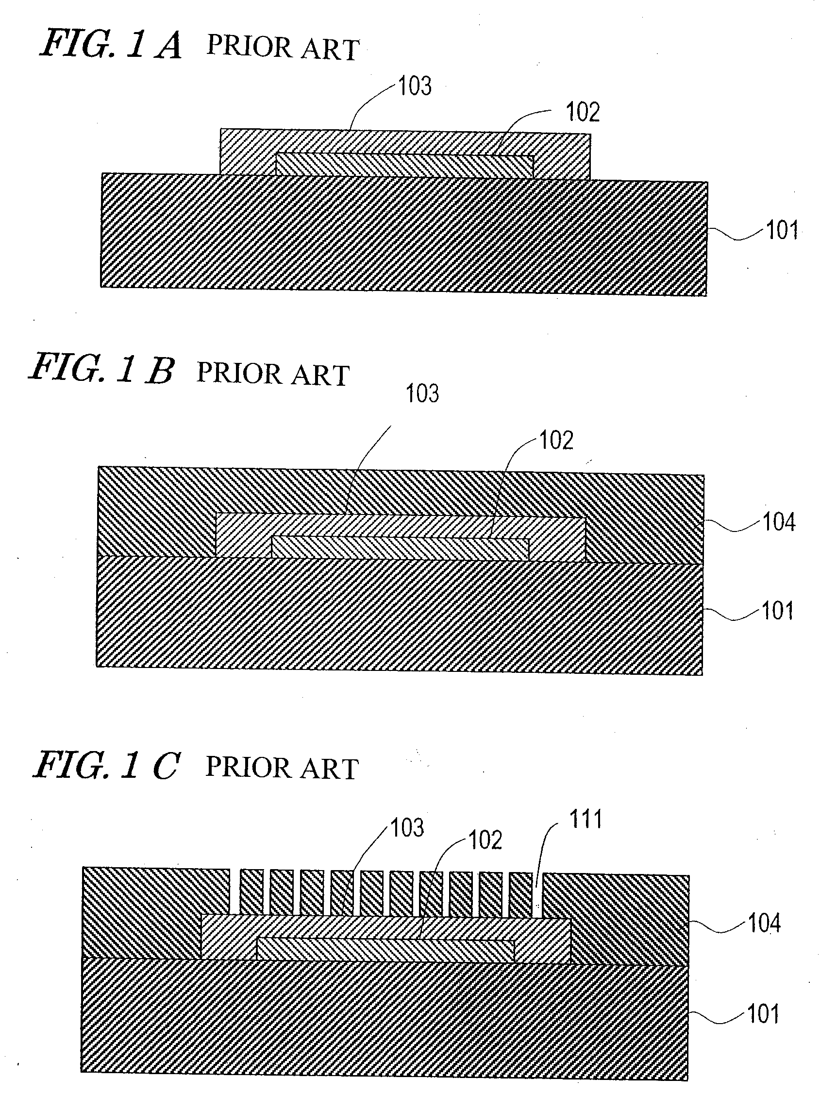
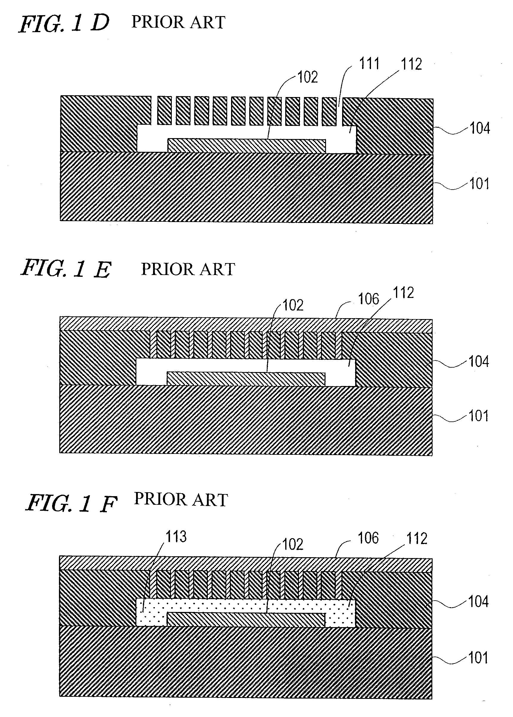
[0182] First, in a step shown in FIG. 4A, a detecting unit 12 such as a bolometer of an infrared sensor is formed on a main face of a silicon substrate 11. Specifically, after a thin film of a material having a sensor function is deposited on the silicon substrate 11, micro-fabrication such as photolithography and etching is performed, thereby patterning the thin film. A planar shape of the detecting unit 12 is designed so as to have the same planar shape as that of the resistive element 151 shown in FIG. 2, for example.
[0183] Next, after a silicon oxide film 13 which covers the detecting unit 12 is deposited on the silicon substrate 11 by a thin film deposition technique such as CVD, the silicon oxide film 13 is patterned so as to cover the detecting unit 12 and the peripheral portion thereof. The patterning can be also performed by photolithography and etching techniqu...
embodiment 2
[0199] Hereinafter a second embodiment according to the present invention will be described.
[0200] In the above-described first embodiment, the etching holes 21 are closed by the metal sealing member 16a by obliquely sputtering a metal from the above of the polysilicon film 14. Alternatively, instead of the oblique sputtering, if the shape of the etching hole 21 is contrived, the etching hole 21 can be closed by vertical sputtering.
[0201] FIGS. 5(a) and (b) are partial sectional views each showing part of a production process of an electronic device according to this embodiment. Both of FIGS. 5(a) and (b) show the configuration of the polysilicon film and the like formed in the step shown in FIG. 4E.
[0202] In the polysilicon film 14 of the electronic device according to a modification shown in FIG. 5(a), an etching hole 21a of a tapered shape is formed. In this modification, the sputtered metal is deposited on a tapered wall of the etching hole 21a, thereby closing the etching ho...
embodiment 3
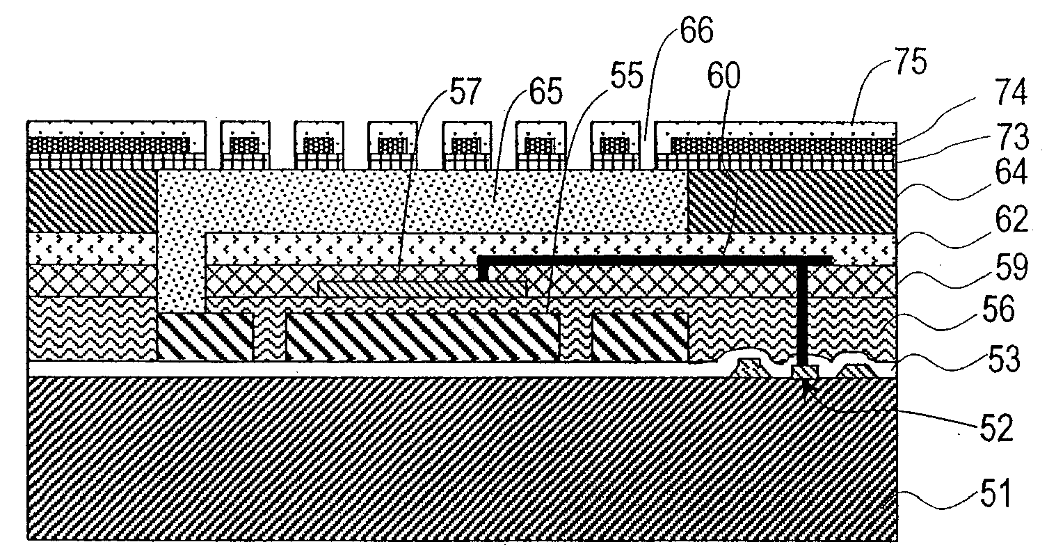
[0208] With reference to FIGS. 7A to 7N, a third embodiment according to the present invention will be described. FIGS. 7A to 7C are sectional views showing steps before a sacrificial layer is formed in a production process of an electronic device in this embodiment. FIGS. 7D to 7F are sectional views showing steps before a BPSG film is planarized after the sacrificial layer is formed in the production process of the electronic device according to this embodiment. FIGS. 7G to 7I are sectional views showing steps before a protection film and the like are patterned after the BPSG film is planarized in the production process of the electronic device according to this embodiment. FIGS. 7J to 7L are sectional views showing steps before etching holes are formed after the protecting film and the like are patterned in the production process of the electronic device according to the embodiment. FIGS. 7M and 7N are sectional views showing steps before a sealing member for closing the etching ...
PUM
 Abstract
Description
Claims
Application Information


