Semiconductor device and method of manufacturing the same

a semiconductor and semiconductor technology, applied in semiconductor devices, semiconductor/solid-state device details, electrical apparatus, etc., can solve the problems of increasing the number of mountings, the wiring flexibility at the time of being mounted to the mounting substrate decreases, and the mounting flexibility can be relatively improved, the effect of increasing general versatility and improving heat radiation efficiency

Inactive Publication Date: 2008-01-17
RENESAS ELECTRONICS CORP
View PDF7 Cites 58 Cited by
  • Summary
  • Abstract
  • Description
  • Claims
  • Application Information

AI Technical Summary

Benefits of technology

[0022]An advantage obtained by typical inventions in inventions disclosed in the application will be briefly explained as follows.
[0023]The first semiconductor chip in which one IGBT is formed and the second semiconductor chip in which one diode is formed are formed in one package, therefore, mounting flexibility can be relatively improved and general versatility can be increased. Since the IGBT and the diode are connected not by wires but the plate electrode (clip), heat radiation efficiency can be improved and on-resistance can be reduced. The current detection circuit and the temperature detection circuit are provided at the IGBT and the diode, thereby detecting overcurrent or abnormal temperature increase to improve reliability of the IGBT and the diode. In addition, the gate electrode for external connection and the electrode for current detection and the electrode for temperature detection are formed at the first edge which is the same side of the emitter electrode for external connection or at the second edge which is opposite to the first edge, therefore, processing in the manufacturing processes is easy and manufacturing costs can be reduced. Moreover, since the plural bonding pads of the first semiconductor chip are formed at the region in which the bonding pads do not overlap with the clip in a flat state, it is possible to prevent wires connecting to the bonding pads from touching the clip. Since the clip can be formed before the wires, it is possible to prevent the wires from having heat load, and to prevent the junction connection of wires from reducing. The position of the second region of the clip between the first semiconductor chip and the second semiconductor chip is apart from the die pad as compared with the position of the first region of the clip which touches the first semiconductor chip or the second semiconductor chip, therefore, short-circuit failure caused by the solder entering to the side surface of the first semiconductor chip or the second semiconductor chip can be reduced.

Problems solved by technology

Therefore, there is a problem that the mount area for IGBTs and diodes becomes large or a problem that the number for mounting processes in which semiconductor devices such as IGBTs and diodes are mounted over a mounting substrate increases.
However, in the semiconductor device in which two IGBTs and two diodes are formed in one package, wiring flexibility at the time of being mounted to the mounting substrate decreases.
The layout structure of the mounting substrate is often changed according to products, and when two IGBTs and two diodes are formed in one package corresponding to each phase, there is a problem that it is difficult to arrange the semiconductor devices efficiently with respect to the change of wiring layout.
In short, there is a problem that mounting flexibility deteriorates.
And further, there is a problem that heating value increases because two IGBTs and two diodes are integrated.
Particularly, the IGBTs and diodes are connected by wires such as gold wires, therefore, there is a problem that heat radiation efficiency is reduced or a problem that on-resistance increases.
In addition, there is a problem that general versatility is insufficient because two IGBT and two diodes are formed in one package.
However, the problem that mounting flexibility deteriorates and the problem that the general versatility deteriorates still exist.

Method used


Image

  • Semiconductor device and method of manufacturing the same
  • Semiconductor device and method of manufacturing the same
  • Semiconductor device and method of manufacturing the same

Examples


embodiment 1

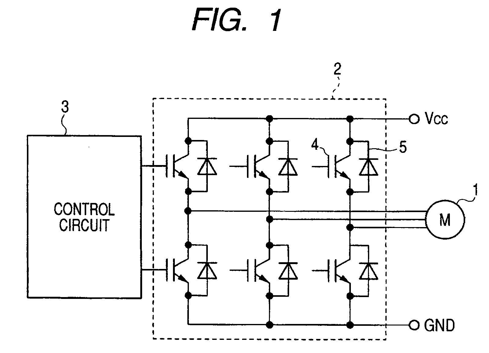
[0085]A semiconductor device in Embodiment 1 is used, for example, to a drive circuit of a three-phase motor applied to a hybrid car and the like. FIG. 1 is a view showing a circuit diagram of a three-phase motor in Embodiment 1. In FIG. 1, the three-phase motor includes a three-phase motor 1, a power semiconductor device 2, and a control circuit 3. The three-phase motor 1 is configured to be driven by three phase voltages of different phases. The power semiconductor device 2 is provided with IGBTs 4 and diodes 5 corresponding to three phases. Specifically, in each single phase, the IGBT 4 and the diode 5 are connected in inverse parallel between the power source potential (Vcc) and the input potential of the three-phase motor, and the IGBT 4 and the diode 5 are connected in inverse parallel also between the input potential of the three-phase motor and the ground potential (GND). That is, two IGBTs 4 and two diodes 5 are provided at each phase, namely, six IGBTs 4 and six diodes 5 a...

embodiment 2

[0154]In Embodiment 2, in the clip to be mounted to the semiconductor chip, an example in which the thickness of portions of the clip touching the semiconductor chip is allowed to be thicker than other portions of the clip will be explained.

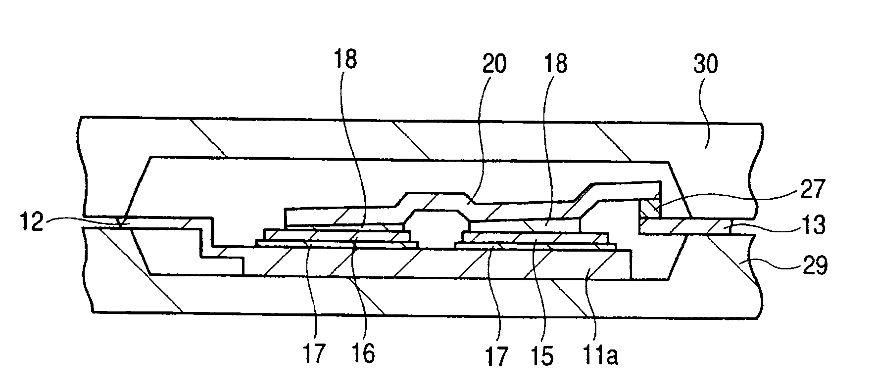
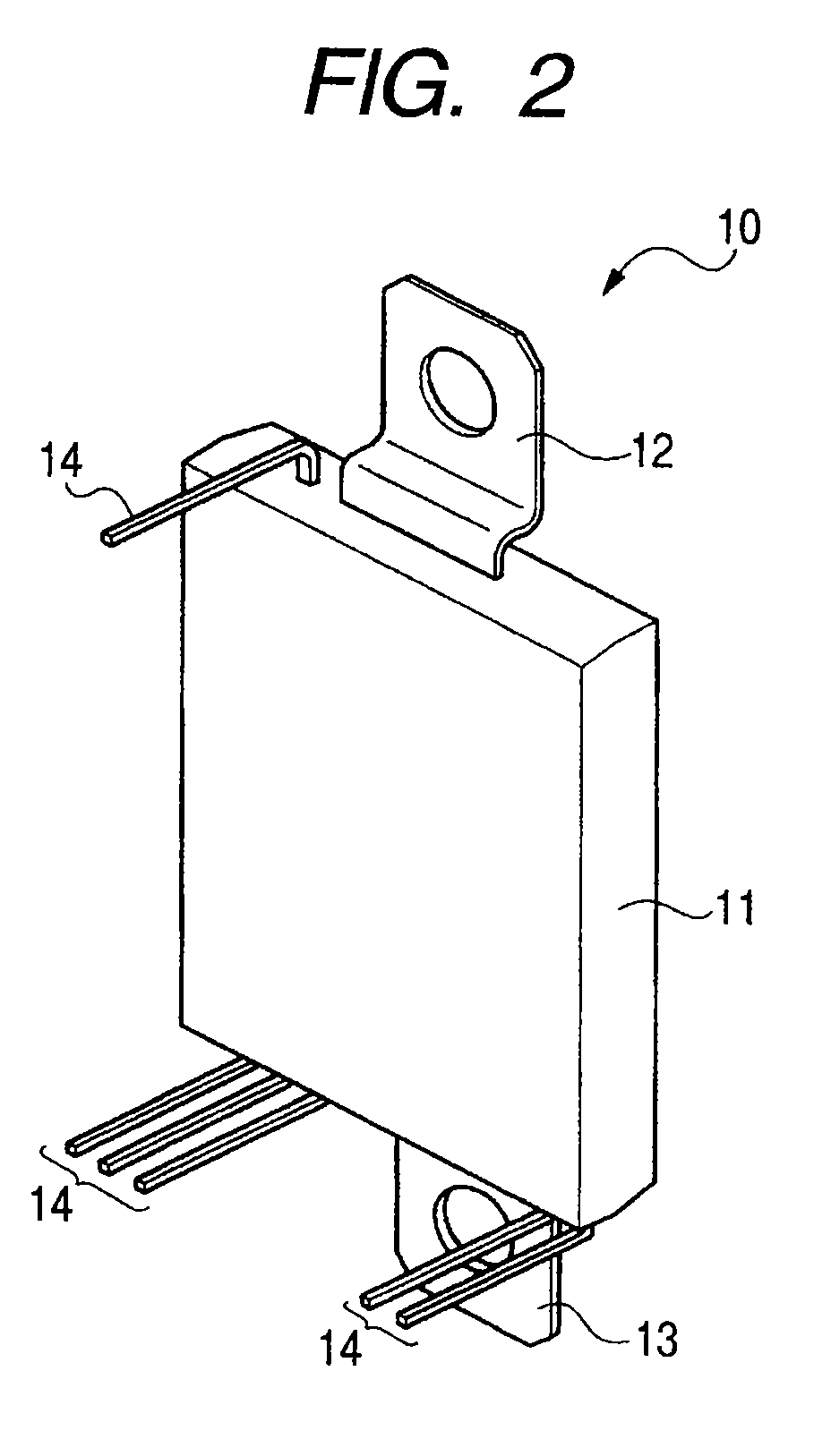
[0155]FIG. 43 is a plan view showing an internal structure of a semiconductor chip 10 in Embodiment 2. The structure shown in FIG. 43 is the same structure as the internal structure of the semiconductor device 10 in Embodiment 1. FIG. 44 is a cross-sectional view showing a cross section taken along an A-A line in FIG. 43. In FIG. 44, a feature of the semiconductor device 10 in Embodiment 2 is in a point in which the shape of a clip 91 is devised. Specifically, the clip 91 is connected to the semiconductor chip 15 and the semiconductor chip 16 through the solder 18, and further, connected to the emitter electrode for external connection 13 through the solder 27. In the clip 91, the thickness of portions touching the semiconductor chip 15 and the s...

embodiment 3

[0156]In Embodiment 3, an example of changing drawing positions of electrodes which are drawn from the resin portion of the semiconductor device will be explained.

[0157]FIG. 45 is a plan view showing an internal structure of the semiconductor device 10 in Embodiment 3. A point in which the semiconductor device 10 shown in FIG. 45 differs from Embodiment 1 is that drawing positions of the collector electrode for external connection 12, the emitter electrode for external connection 13, the electrodes for temperature detection 21, 22, the gate electrode for external connection 23, the electrode for Kelvin detection 24, the electrode for current detection 25 and the electrode for Kelvin detection 26 are different. In Embodiment 1, these electrodes are formed at the short edge sides of the die pad 11a whose planar shape is a rectangle shape. In Embodiment 3, these electrodes are formed at two edges at the long edge sides of the die pad 11a, which is opposite to each other. Specifically, ...


PUM


Abstract

A semiconductor device is provided, which is capable of improving mounting flexibility relatively and increasing general versatility, as well as realizing heat radiation characteristics and low on-resistance. Moreover, the semiconductor device is provided, which is capable of improving reliability, performing processing in manufacturing processes easily and reducing manufacturing costs. Also, the semiconductor device capable of decreasing the mounting area is provided. A semiconductor chip in which an IGBT is formed and a semiconductor chip in which a diode is formed are mounted over a die pad. Then, the semiconductor chip and the semiconductor chip are connected by using a clip. The clip is arranged so as not to overlap with bonding pads formed at the semiconductor chip in a flat state. The bonding pads formed at the semiconductor chip are connected to electrodes by using wires.

Description

CROSS-REFERENCE TO RELATED APPLICATIONS[0001]The disclosure of Japanese Patent Application No. 2006-191830 filed on Jul. 12, 2006 including the specification, drawings and abstract is incorporated herein by reference in its entirety.BACKGROUND OF THE INVENTION[0002]1. Field of the Invention[0003]The invention relates to a semiconductor device and a manufacturing technology of the same, for example, relates to a technology which is effective when applied to a semiconductor device and manufacture thereof used for on-vehicle motor control.[0004]2. Background Art[0005]In Japanese patent laid-open No. 2005-243685 (Patent Document 1), a semiconductor device in which one IGBT (Insulated Gate Bipolar Transistor) is formed in one package is disclosed.[0006]In Japanese patent laid-open No. 2004-47850 (Patent Document 2), a structure in which two IGBTs and two diodes are formed in one package and a wire is not used for connection between IGBTs and diodes is disclosed.[0007]In Japanese patent l...

Claims


Application Information

Patent Timeline
Patent Type & Authority Applications(United States)
IPC IPC(8): H01L31/111H01L21/00
CPCH01L21/565H01L23/49524H01L2924/1305H01L2224/40137H01L2224/37147H01L2224/40247H01L2224/73221H01L24/49H01L2924/01047H01L2924/01033H01L2924/01019H01L2924/01006H01L23/49562H01L23/49575H01L24/36H01L24/40H01L24/45H01L2224/45124H01L2224/45144H01L2224/48247H01L2224/49171H01L2924/01002H01L2924/01004H01L2924/01013H01L2924/01014H01L2924/01015H01L2924/01029H01L2924/0105H01L2924/01051H01L2924/01078H01L2924/01079H01L2924/01082H01L2924/13055H01L2924/30107H01L24/48H01L2924/01005H01L2924/00014H01L2924/00H01L2924/181H01L2224/40095H01L2224/40139H01L2924/12036H01L24/37H01L2224/05553H01L2224/84801H01L2224/83801H01L2224/0603H01L24/84H01L2924/19107H01L2924/00012
Inventor MUTO, AKIRASHIMIZU, ICHIOILJIMA, TETSUOHATA, TOSHIYUKIISHIZAKA, KATSUO
Owner RENESAS ELECTRONICS CORP
Why Eureka
Try Eureka