

Switching circuit and driving circuit for transistor
a technology of switching circuit and driving circuit, which is applied in the direction of pulse generator, pulse manipulation, pulse technique, etc., can solve the problems of low on-state resistance of transistors and small number of parts for providing circuits, and achieve small surge voltage and small switching loss.
- Summary
- Abstract
- Description
- Claims
- Application Information
AI Technical Summary
Benefits of technology
Problems solved by technology
Method used
Image

Examples
first embodiment
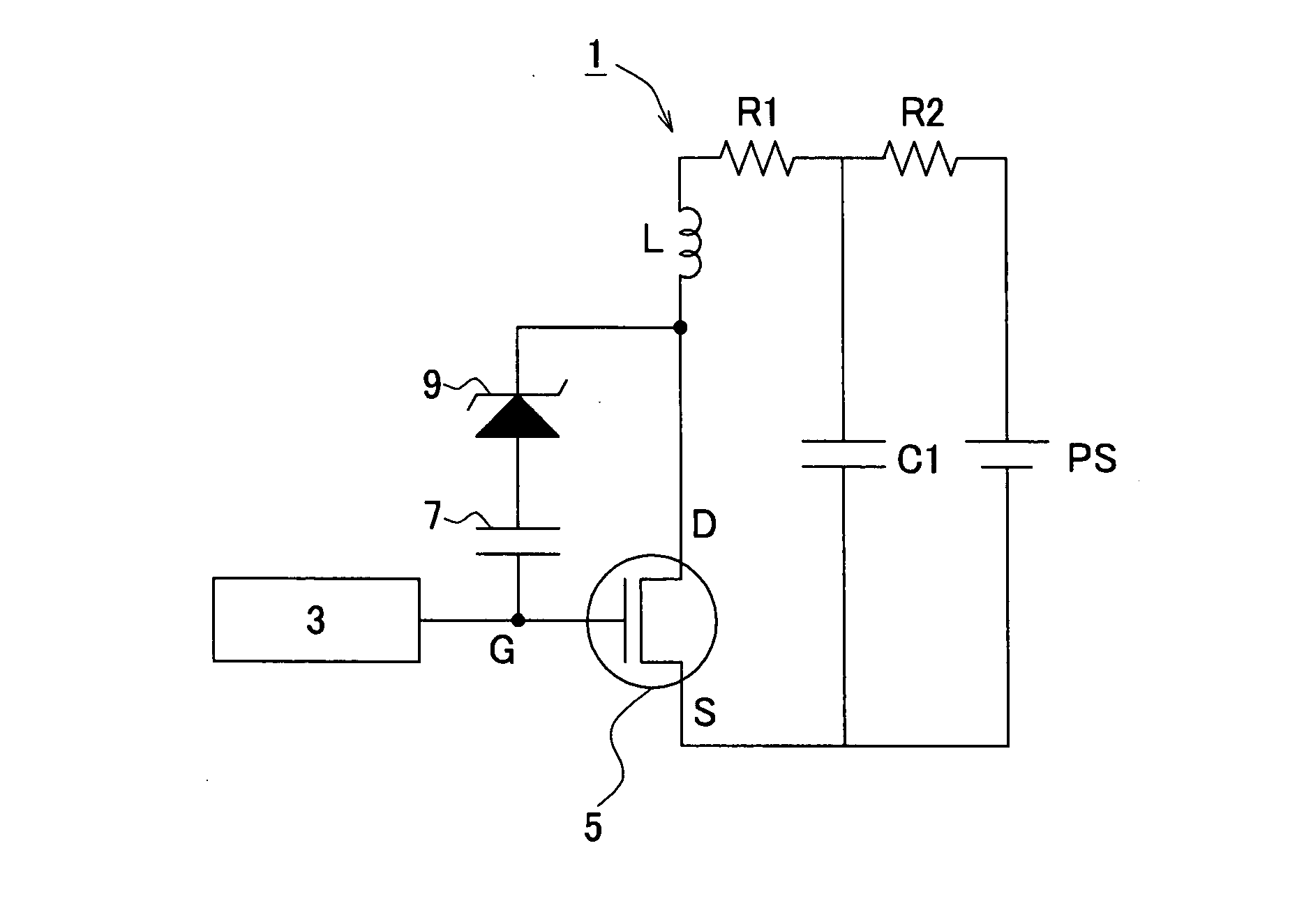
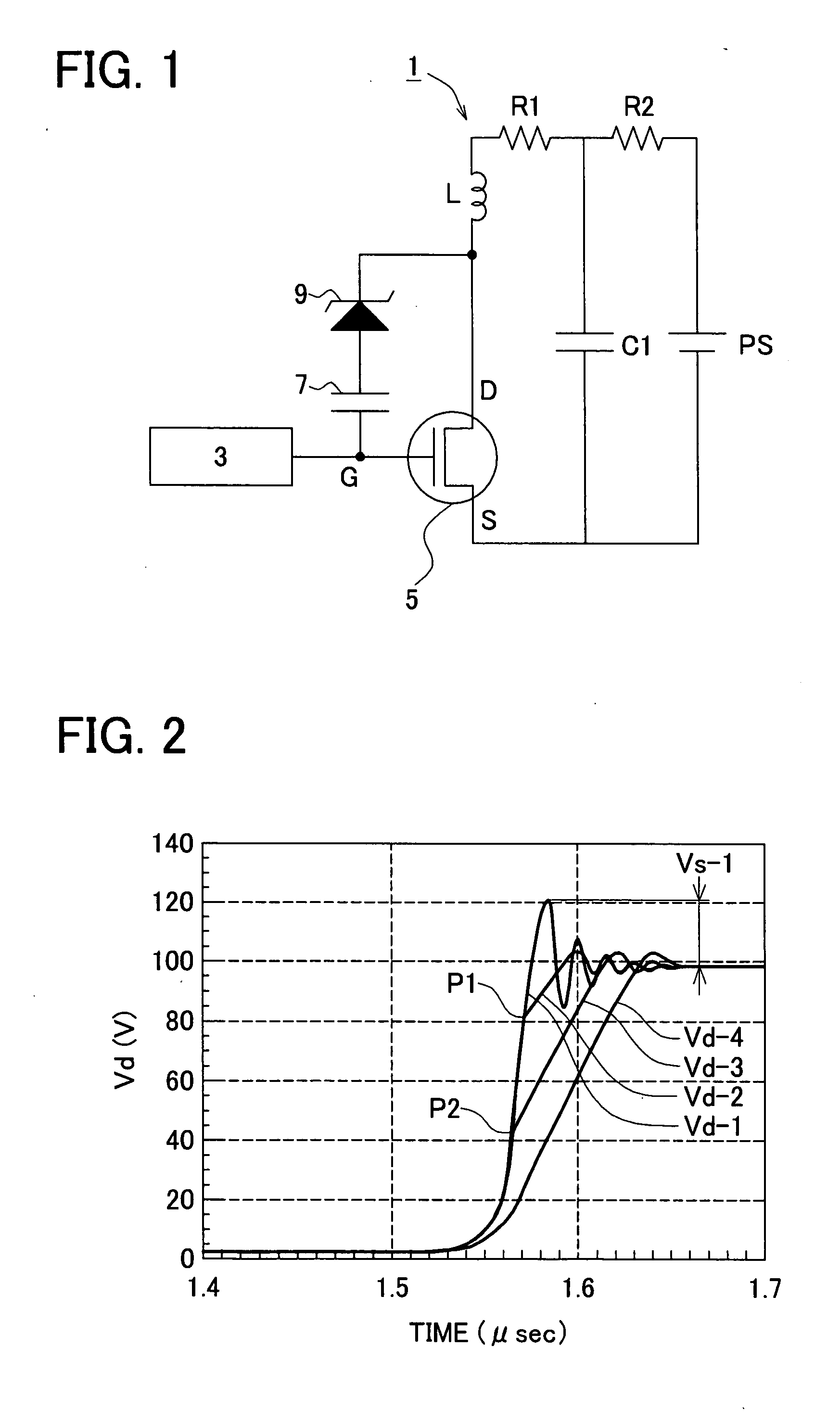
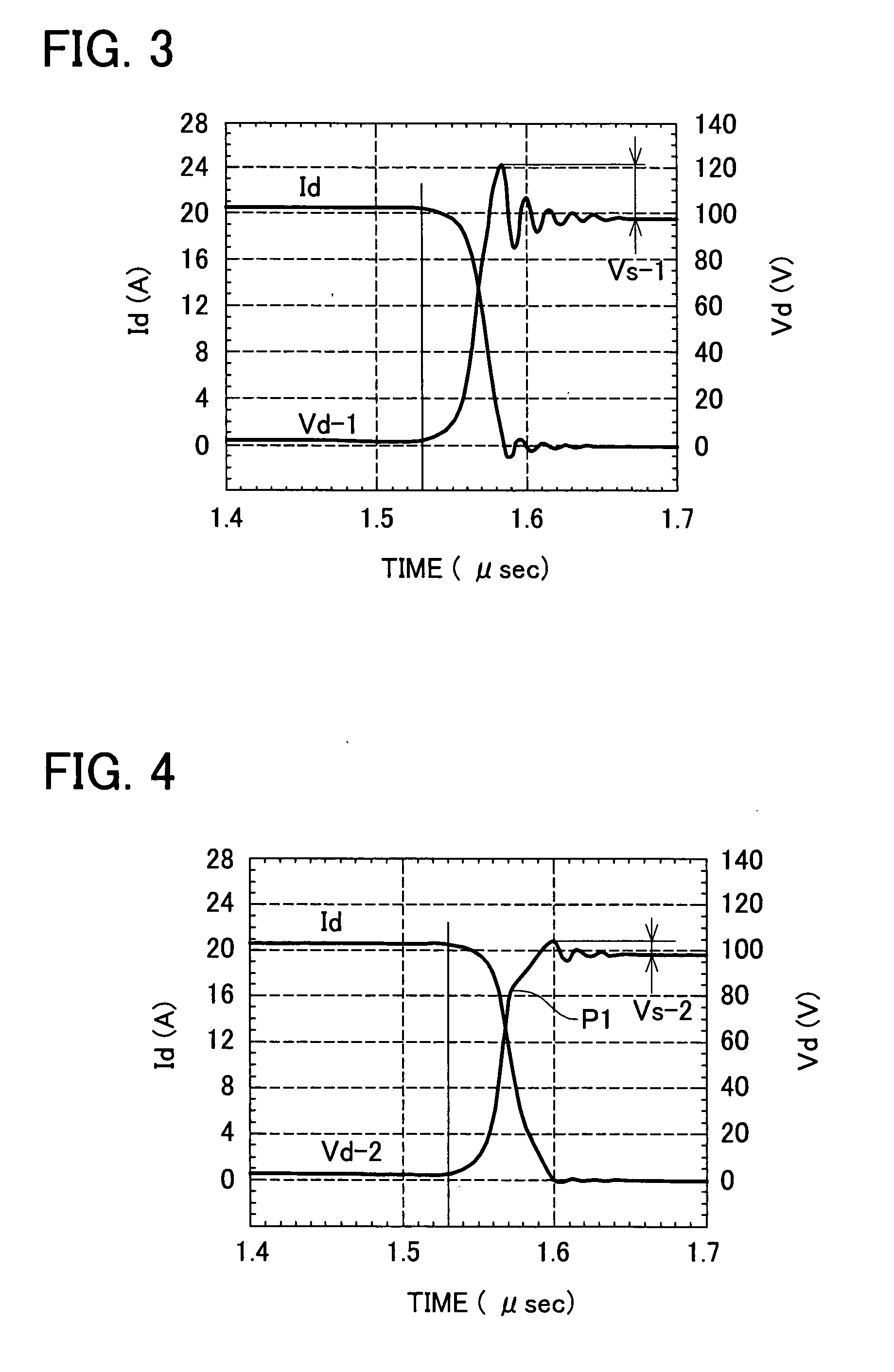
[0138]FIG. 1 shows a major portion of a switching circuit 1 according to a first embodiment of the present disclosure. The switching circuit 1 has been equipped with a DC power supply PS, a load resistor R1, and a transistor (namely, MOSFET) 5, while these circuit elements has been series-connected to each other. The switching circuit 1 has also be equipped with a capacitance component C1, a resistance component R2, and a stray inductance component L which is caused by a wiring line, and the like. When a current flowing between main electrodes (namely, drain D and source S) of the transistor 5 is rapidly changed by the stray inductance component L, a large surge voltage is generated between the major electrodes of the transistor 5, and thus, there are some possibilities that this large surge voltage may damage the transistor 5, or may become noise which may give an adverse influence to other appliances.
[0139] The transistor 5 is a unipolar type transistor, while a drain D thereof h...
second embodiment
[0168]FIG. 7 shows a major portion of a switching circuit 10 according to a second embodiment of the present disclosure. The switching circuit 10 has been equipped with a DC power supply PS, a load resistor R1, and a transistor (namely, MOSFET) 5, while these circuit elements has been series-connected to each other. The switching circuit 10 has also be equipped with a capacitance component C1, a resistance component R2, and a stray inductance component L which is caused by a wiring line, and the like. When a current flowing between main electrodes (namely, drain D and source S) of the transistor 5 is rapidly changed by the stray inductance component L, a large surge voltage is generated between the major electrodes of the transistor 5, and thus, there are some possibilities that this large surge voltage may damage the transistor 5, or may become noise which may give an adverse influence to other appliances.
[0169] The transistor 5 is a unipolar type transistor, while a drain D there...
third embodiment
[0200]FIG. 12A to FIG. 16B indicate examples in which transistors, zener diodes 9, and capacitors 7, which have been employed in switching circuits, have been formed on the same semiconductor substrate 20. Any of the examples shown in FIG. 12A to FIG. 16B are to embody the portions of the transistor, the zener diode 9, and the capacitor 7 employed in the switching circuit 1 of the first embodiment. Any of these examples shown in FIG. 12A to FIG. 16B corresponds to such a semiconductor mode that while the transistor and the capacitor 7 have been formed in the semiconductor substrate 20, the zener diode 9 has been provided on the semiconductor substrate 20. The transistor, the zener diode 9, and the capacitor 7 have been formed in an integral body by utilizing the semiconductor substrate 20, and have been constituted in a single chip. It should also be understood that single crystal silicon has been employed in the semiconductor substrate 20.
[0201] The semiconductor mode shown in FIG...
PUM
 Abstract
Description
Claims
Application Information