Eureka AIR delivers breakthrough ideas for toughest innovation challenges, trusted by R&D personnel around the world.

Switching circuit and driving circuit for transistor

a technology of switching circuit and driving circuit, which is applied in the direction of pulse generator, pulse manipulation, pulse technique, etc., can solve the problems of low on-state resistance of transistors and small number of parts for providing circuits, and achieve small surge voltage and small switching loss.

Inactive Publication Date: 2010-03-02
DENSO CORP
View PDF28 Cites 3 Cited by
  • Summary
  • Abstract
  • Description
  • Claims
  • Application Information

AI Technical Summary

Benefits of technology

[0043]In view of the above-described problem, it is an object of the present invention to provide a switching circuit having a small switching loss and a small surge voltage. It is another object of the present invention to provide a driving circuit for a transistor.
[0045]In the above switching circuit, the switching loss can be reduced. Further, the surge voltage also can be reduced. Accordingly, both of the switching loss and the surge voltage are limited to be small. Furthermore, the transistor has a low on-state resistance (or, a low on-state voltage), and the number of parts for providing the circuit is small.
[0049]In the above circuit, by utilizing the voltage control circuit, a timing for slowing a changing speed of a voltage generated in the control electrode of the transistor is controlled when the transistor is turned off. When this timing is adjusted earlier, the surge voltage can be reduced. Further, in the above circuit, since the changing speed of the voltage generated in the control electrode of the transistor is slowed during the transistor is turning off, both of the turn-off loss and the surge voltage are reduced.
[0051]In the above circuit, the surge voltage of the switching circuit including the transistor is accurately and stably reduced.
[0053]In the above circuit, the surge voltage of the switching circuit including the transistor is accurately and stably reduced.
[0055]In the above driving circuit, there is no need to have a circuit for setting a threshold accurately, similar to on / off operation of a semiconductor switching element. Accordingly, the construction of the above driving circuit is simplified. In the above driving circuit, a width of the current path of the variable resistor is controlled by utilizing the depletion layer, which is expandable in accordance with the voltage between the main electrodes of the transistor. Further, the construction of the circuit is simplified, and a manufacturing cost of the circuit is also reduced.

Problems solved by technology

Furthermore, the transistor has a low on-state resistance (or, a low on-state voltage), and the number of parts for providing the circuit is small.

Method used


Image

  • Switching circuit and driving circuit for transistor
  • Switching circuit and driving circuit for transistor
  • Switching circuit and driving circuit for transistor

Examples


first embodiment

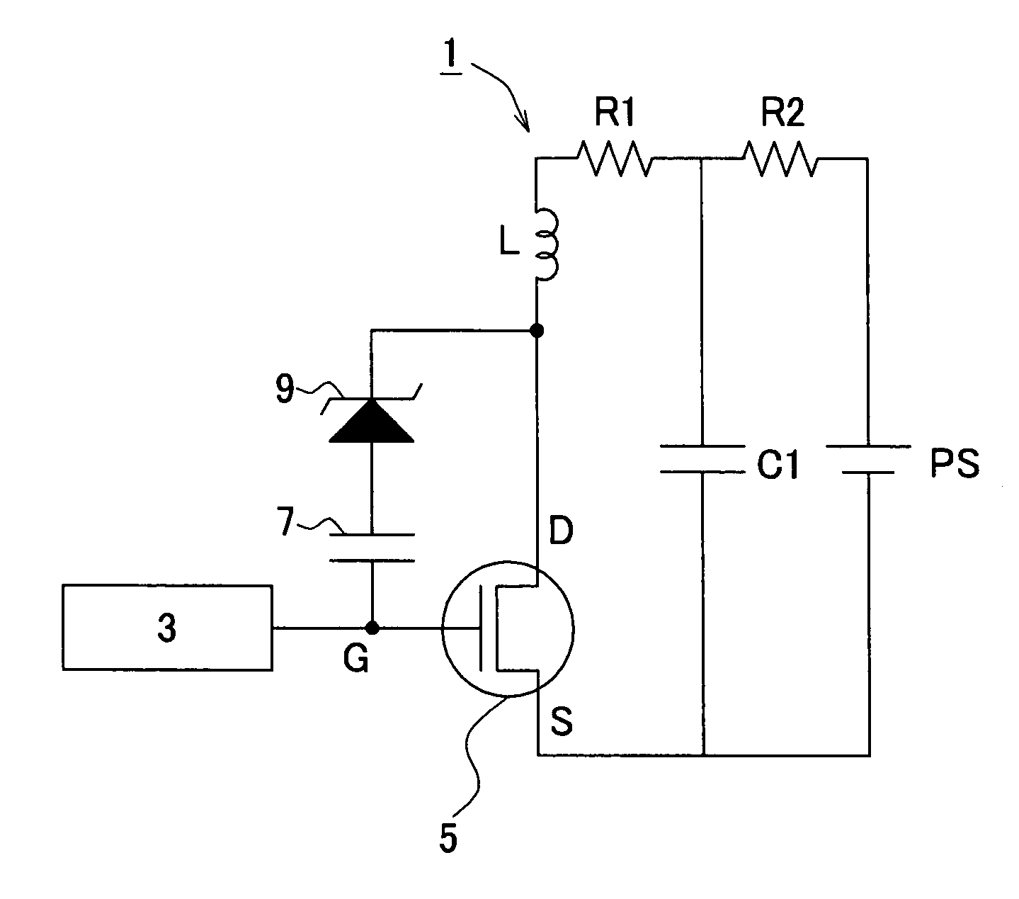
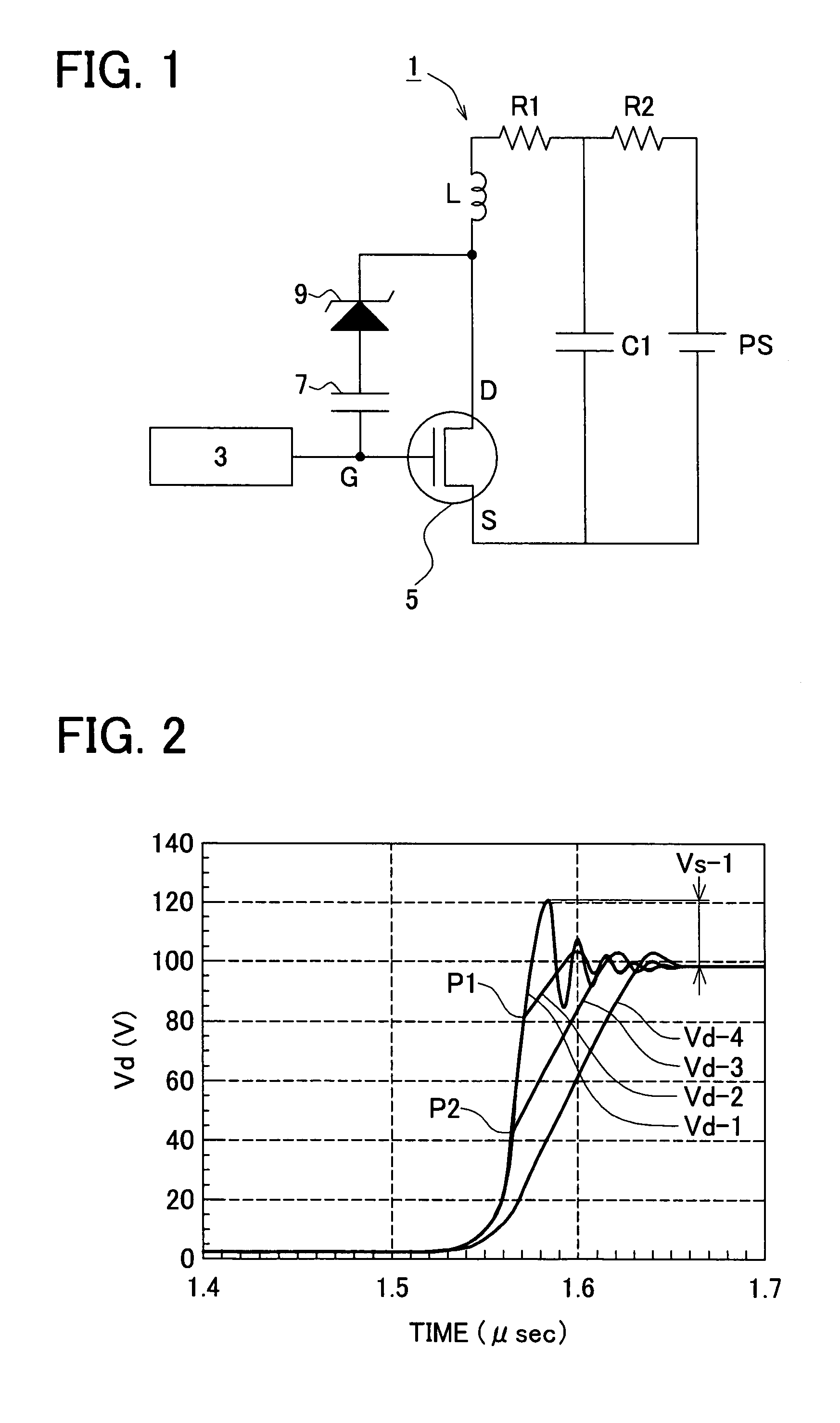
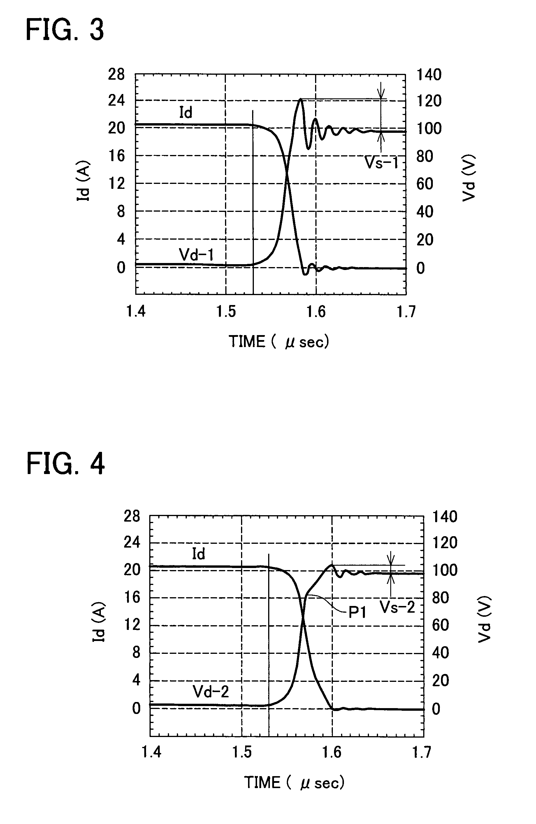
[0138]FIG. 1 shows a major portion of a switching circuit 1 according to a first embodiment of the present disclosure. The switching circuit 1 has been equipped with a DC power supply PS, a load resistor R1, and a transistor (namely, MOSFET) 5, while these circuit elements has been series-connected to each other. The switching circuit 1 has also be equipped with a capacitance component C1, a resistance component R2, and a stray inductance component L which is caused by a wiring line, and the like. When a current flowing between main electrodes (namely, drain D and source S) of the transistor 5 is rapidly changed by the stray inductance component L, a large surge voltage is generated between the major electrodes of the transistor 5, and thus, there are some possibilities that this large surge voltage may damage the transistor 5, or may become noise which may give an adverse influence to other appliances.

[0139]The transistor 5 is a unipolar type transistor, while a drain D thereof has...

second embodiment

[0168]FIG. 7 shows a major portion of a switching circuit 10 according to a second embodiment of the present disclosure. The switching circuit 10 has been equipped with a DC power supply PS, a load resistor R1, and a transistor (namely, MOSFET) 5, while these circuit elements has been series-connected to each other. The switching circuit 10 has also be equipped with a capacitance component C1, a resistance component R2, and a stray inductance component L which is caused by a wiring line, and the like. When a current flowing between main electrodes (namely, drain D and source S) of the transistor 5 is rapidly changed by the stray inductance component L, a large surge voltage is generated between the major electrodes of the transistor 5, and thus, there are some possibilities that this large surge voltage may damage the transistor 5, or may become noise which may give an adverse influence to other appliances.

[0169]The transistor 5 is a unipolar type transistor, while a drain D thereof...

third embodiment

[0200]FIG. 12A to FIG. 16B indicate examples in which transistors, zener diodes 9, and capacitors 7, which have been employed in switching circuits, have been formed on the same semiconductor substrate 20. Any of the examples shown in FIG. 12A to FIG. 16B are to embody the portions of the transistor, the zener diode 9, and the capacitor 7 employed in the switching circuit 1 of the first embodiment. Any of these examples shown in FIG. 12A to FIG. 16B corresponds to such a semiconductor mode that while the transistor and the capacitor 7 have been formed in the semiconductor substrate 20, the zener diode 9 has been provided on the semiconductor substrate 20. The transistor, the zener diode 9, and the capacitor 7 have been formed in an integral body by utilizing the semiconductor substrate 20, and have been constituted in a single chip. It should also be understood that single crystal silicon has been employed in the semiconductor substrate 20.

[0201]The semiconductor mode shown in FIG. ...


PUM


Abstract

A switching circuit includes: a transistor having a first electrode, a second electrode and a control electrode; a zener diode; and a capacitor. A connection between the first electrode and the second electrode is capable of temporally switching between a condition state and a non-conduction state by switching a control voltage of the transistor. The zener diode and the capacitor are coupled in series between the first electrode and the control electrode of the transistor. The first electrode is a drain or a collector.

Description

CROSS REFERENCE TO RELATED APPLICATIONS[0001]This application is based on Japanese Patent Applications No. 2006-79382 filed on Mar. 22, 2006, No. 2006-86225 filed on Mar. 27, 2006, No. 2006-204769 filed on Jul. 27, 2006, No. 2006-204770 filed on Jul. 27, 2006, No. 2006-243832 filed on Sep. 8, 2006, No. 2007-73381 filed on Mar. 20, 2007, No. 2007-73382 filed on Mar. 20, 2007, and No. 2007-74030 filed on Mar. 22, 2007, the disclosures of which are incorporated herein by reference.FIELD OF THE INVENTION[0002]The present invention relates to a switching circuit and a driving circuit for a transistor.BACKGROUND OF THE INVENTION[0003]Switching circuits have been widely utilized in DC-DC converters, inverters, or the like. There are many possibilities that typical switching circuits utilize transistors such as MOSFETs, IGBTs, or the like. In switching circuits, since voltages applied to gates of transistors are switched, signal paths between major electrodes (namely, sources and drains in ...

Claims


Application Information

Patent Timeline
Patent Type & Authority Patents(United States)
IPC IPC(8): H03K3/00
CPCH01L27/0255H01L27/0629H03K17/063H03K17/168H03K17/567H03K17/687H03K17/165H03K2217/0036
Inventor AOKI, TAKAAKIMIZUNO, SHOJITAKAHASHI, SHIGEKINAKANO, TAKASHIAKAGI, NOZOMUHATTORI, YOSHIYUKIKUWAHARA, MAKOTOOKADA, KYOKO
Owner DENSO CORP
Why Eureka
Eureka Blog
Learn More