Method Of Manufacturing A Hollow Circuit Substrate

Inactive Publication Date: 2008-01-17
NEC CORP +1
View PDF7 Cites 13 Cited by
  • Summary
  • Abstract
  • Description
  • Claims
  • Application Information

AI Technical Summary

Benefits of technology

[0034] According to the method of manufacturing a hollow circuit substrate as described above in (4), a flux film which is formed by application of a flux suspension can be uniformly formed with a thin film thickness. Accordingly, falling off of flux after coating can be prevented. If the film thickness of a flux film is thick, there is the possibility of its falling off due to even a slight impact or under handling, and there is the possibility of problems developing with respect to the ease of brazing or the external appearance after brazing. In addition, the adhered amount of flux can be made small, so it has the effect of preventing plugging up of a circuit and of improving the external appearance

Problems solved by technology

However, in recent electronic equipment, due to miniaturization and increases in performance, there is a tendency for the amount of heat which is generated by heat dissipating electronic parts to increase, and a sufficient heat generating performance can no longer be obtained by conventional methods.
In addition, in notebook personal computers, two-dimensional display apparatuses, projectors, and the like, the noise generated by cooling fans is increasing, and it is not possible to provide the quietness which has come to be demanded of this equipment.
However, in the liquid cooling system described in the publication, heat is dissipated only from the cooling liquid circulating tube, so the heat dissipating surface area is insufficient, and it has the problem that its heat dissipating efficiency is poor.
However, with these coating methods, it is difficult to apply a flux suspension only to necessary portions, and excessive amount

Method used


Image

  • Method Of Manufacturing A Hollow Circuit Substrate
  • Method Of Manufacturing A Hollow Circuit Substrate
  • Method Of Manufacturing A Hollow Circuit Substrate

Examples


Example

[0042] Below, embodiments of this invention will be explained while referring to the drawings.

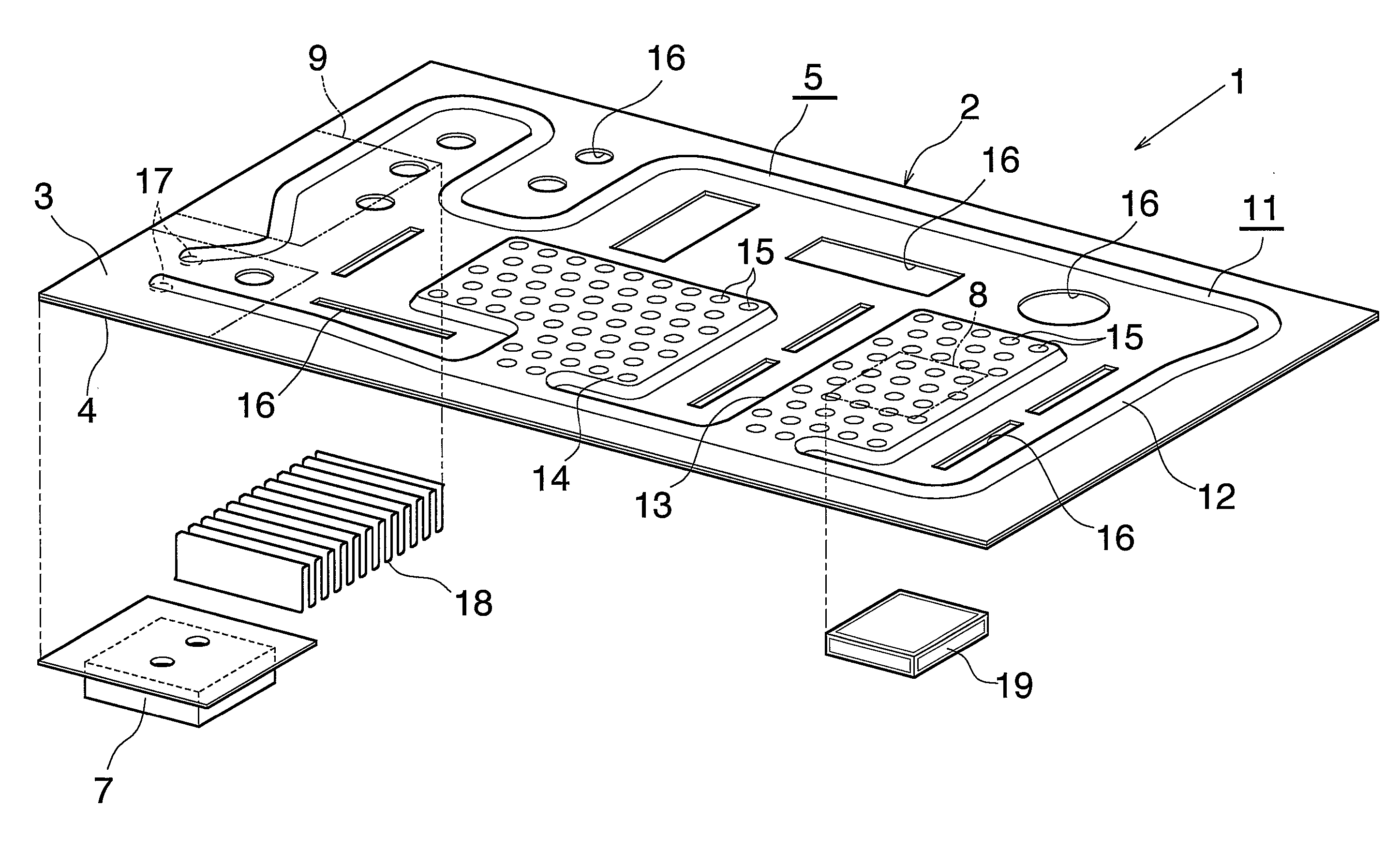
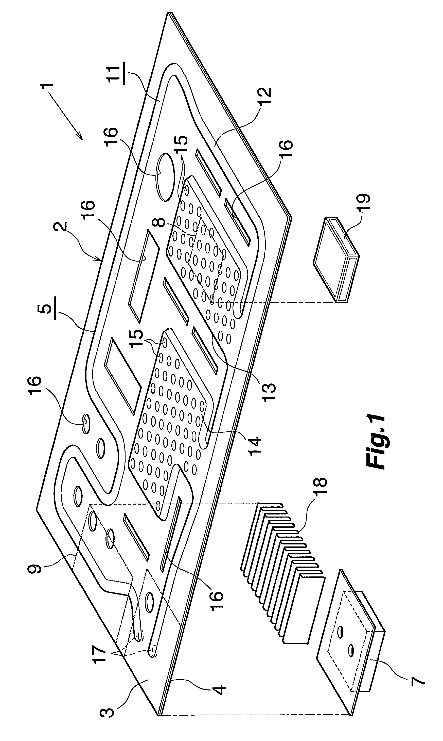
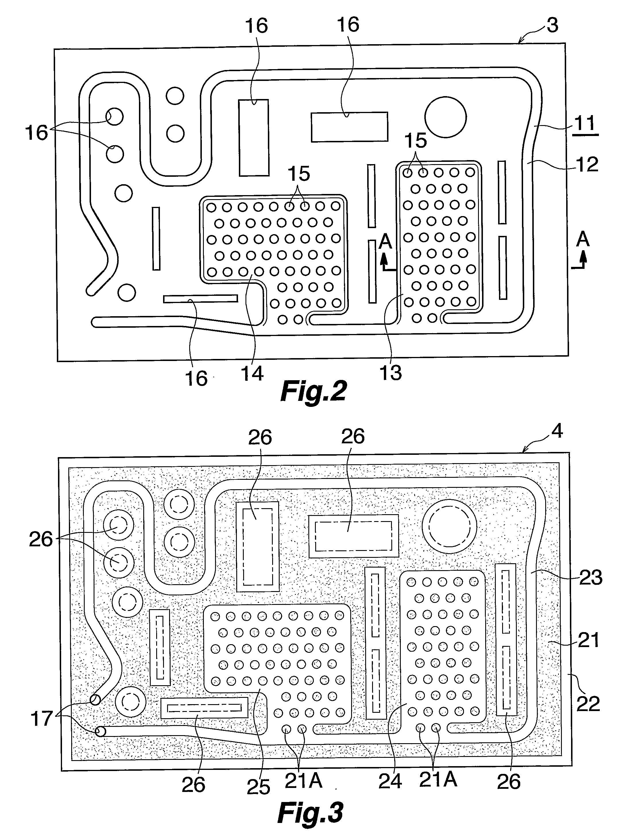
[0043]FIG. 1 shows the overall structure of a liquid-cooled heat dissipating apparatus using a hollow circuit substrate manufactured by a method according to this invention, and FIG. 2 to FIG. 4 show a method of manufacturing a hollow circuit substrate.

[0044] In FIG. 1, a liquid-cooled heat dissipating apparatus 1 has a planar hollow circuit substrate 2 made from an upper and lower sheet with a high thermal conductivity which are joined to each other in a laminated state and which in this case are aluminum metal sheets 3 and 4. A cooling fluid circulating passage 5 is formed between the metal sheets 3 and 4 of the hollow circuit substrate 2 as a hollow circuit.

[0045] A cooling fluid, such as antifreeze, which is not corrosive with respect to aluminum is sealed inside the cooling fluid circulating passage 5 in the hollow circuit substrate 2. The cooling fluid is circulated inside the flui...


PUM

PropertyMeasurementUnit
Percent by massaaaaaaaaaa
Particle diameteraaaaaaaaaa
Concentrationaaaaaaaaaa

Abstract

A method of manufacturing a hollow circuit substrate, of two metal sheets brazed to each other in a laminated state with a bulging hollow circuit for ed between the two metal sheets. Of the upper and lower metal sheets for forming the hollow circuit, a circuit-forming bulging portion is formed in the upper metal sheet. A flux suspension is applied by screen printing to the upper surface of the lower metal sheet so as not to overlap the circuit-forming bulging portion to form flux films. The two metal sheets are stacked on each other so as to close off the opening of the circuit-forming bulging portion and are brazed to each other. This method prevents flux from remaining in a hollow circuit of a manufactured hollow circuit substrate.

Description

CROSS REFERENCE TO RELATED APPLICATIONS [0001] This application is an application filed under 35 U.S.C. §111(a) claiming the benefit pursuant to 35 U.S.C. §119(e)(1) of the filing date of Provisional Application No. 60 / 619,034 filed Oct. 18, 2004 pursuant to 35 U.S.C. §111(b).TECHNICAL FIELD [0002] This invention relates to a method of manufacturing a hollow circuit substrate. More particularly, it relates to a method of manufacturing a hollow circuit substrate which is used in a liquid-cooled heat dissipating apparatus for dissipating heat which is generated by heat generating bodies such as heat generating electronic components of electronic equipment such as notebook personal computers, two-dimensional display apparatuses, and projectors, or which is used in planar heat pipes used for cooling heat generating electronic parts such as IPM (intelligent power modules), IGBT (insulated gate bipolar transistors), and thyristors. [0003] In this specification and in the claims, the term ...

Claims


Application Information

Patent Timeline
IPC IPC(8): H05K7/20
CPCB23K1/0012B23K2201/14B23K2201/40B23K2203/10Y10T29/4935H01L23/473H01L2924/0002H01L23/427H01L2924/00F28F3/14B23K2101/14B23K2101/40B23K2103/10
Inventor UEDA, MASAFUMIKONDOU, MIKIOIKAWA, YOHEI
Owner NEC CORP
Why Eureka
Try Eureka