
Display and method for manufacturing display

a technology of display and display screen, applied in the field of display, can solve the problems of large error amount between the target film thickness and the film thickness actually deposited, and is susceptible to external damage, and achieve the effects of preventing the occurrence of defective spots in the first organic electroluminescent element, and reducing the risk of damag

Inactive Publication Date: 2008-01-24
SONY CORP
View PDF15 Cites 64 Cited by
  • Summary
  • Abstract
  • Description
  • Claims
  • Application Information

AI Technical Summary

Benefits of technology

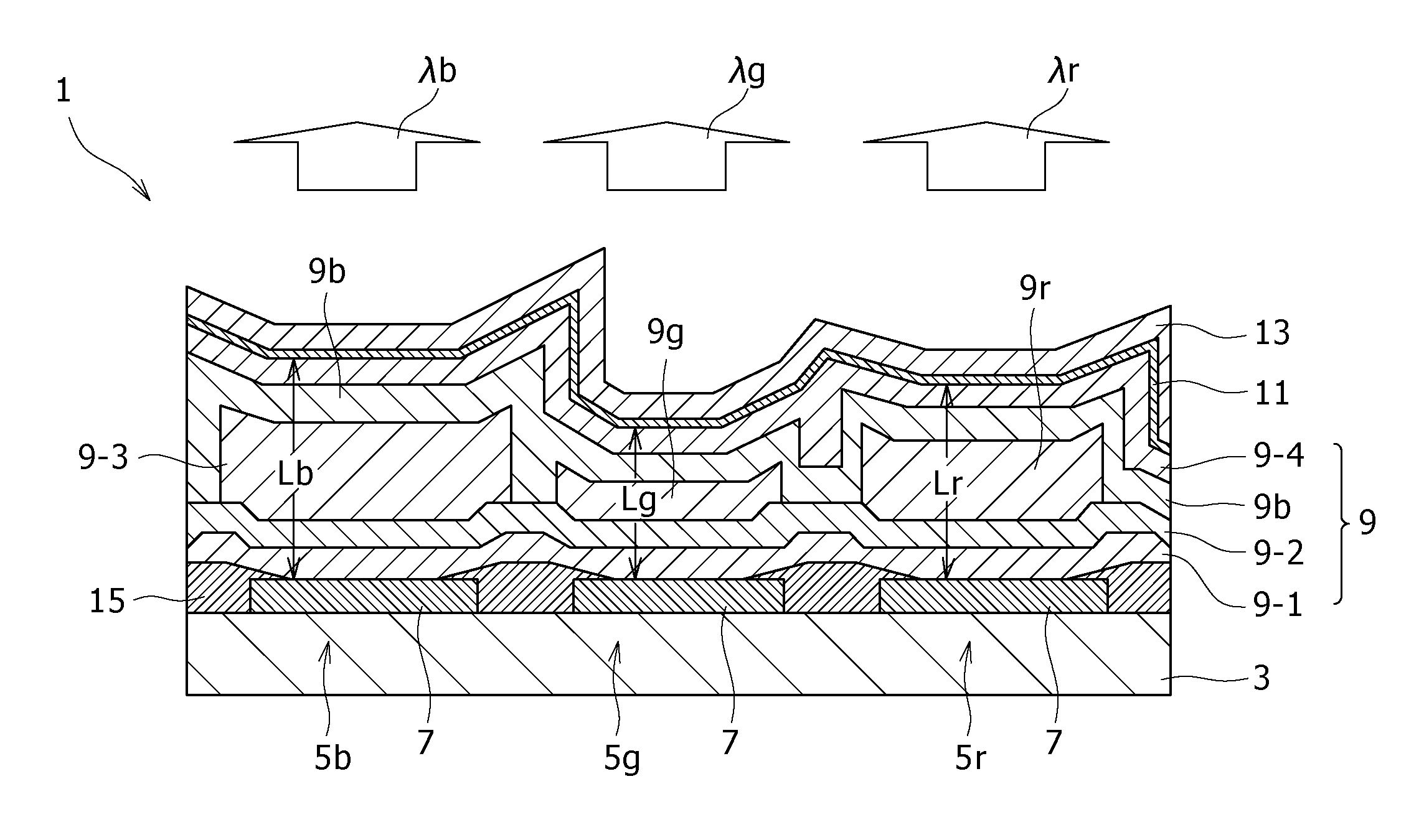
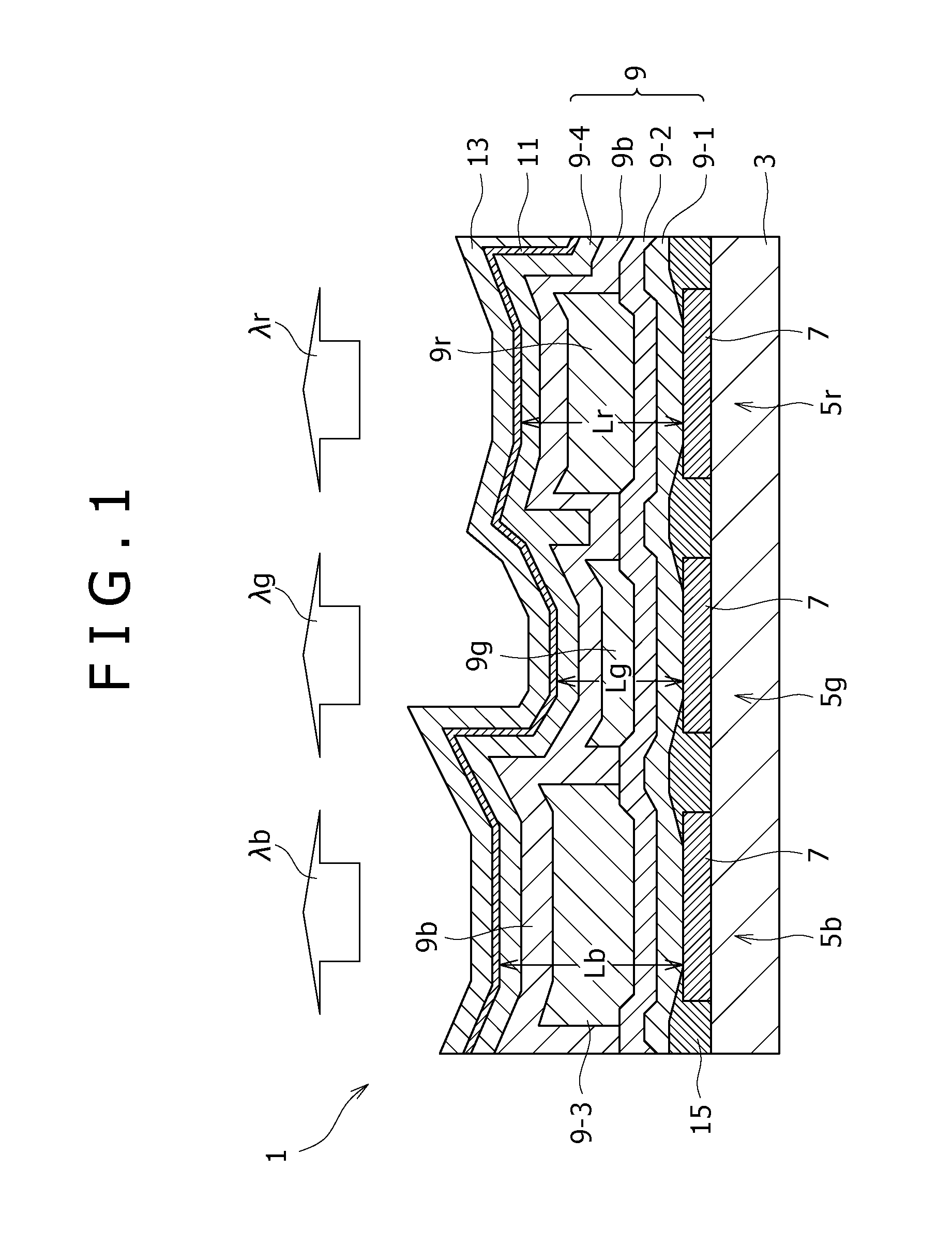
The present invention provides a full-color display with organic electroluminescent elements that have reduced defective spots and controlled light emission characteristics. This is achieved by adjusting the film thickness of the organic layer in the organic electroluminescent elements to resonance with the wavelength of the luminescent light generated in the light-emitting layer. In particular, the film thickness of the organic layer in the first organic electroluminescent element that generates first color luminescent light is set larger than the film thickness of the organic layer in the second organic electroluminescent element that generates second color luminescent light. This prevents defective spots in the first organic electroluminescent element and ensures the controllability of light emission characteristics. The method for manufacturing the display is also provided.

Problems solved by technology

However, if the film thicknesses of the organic layers of the respective colors are designed to follow the order of the wavelengths of emitted light as described above, the organic layer of B, of which wavelength of emitted light is the shortest, is formed as the thinnest film, and thus is susceptible to the external damage.
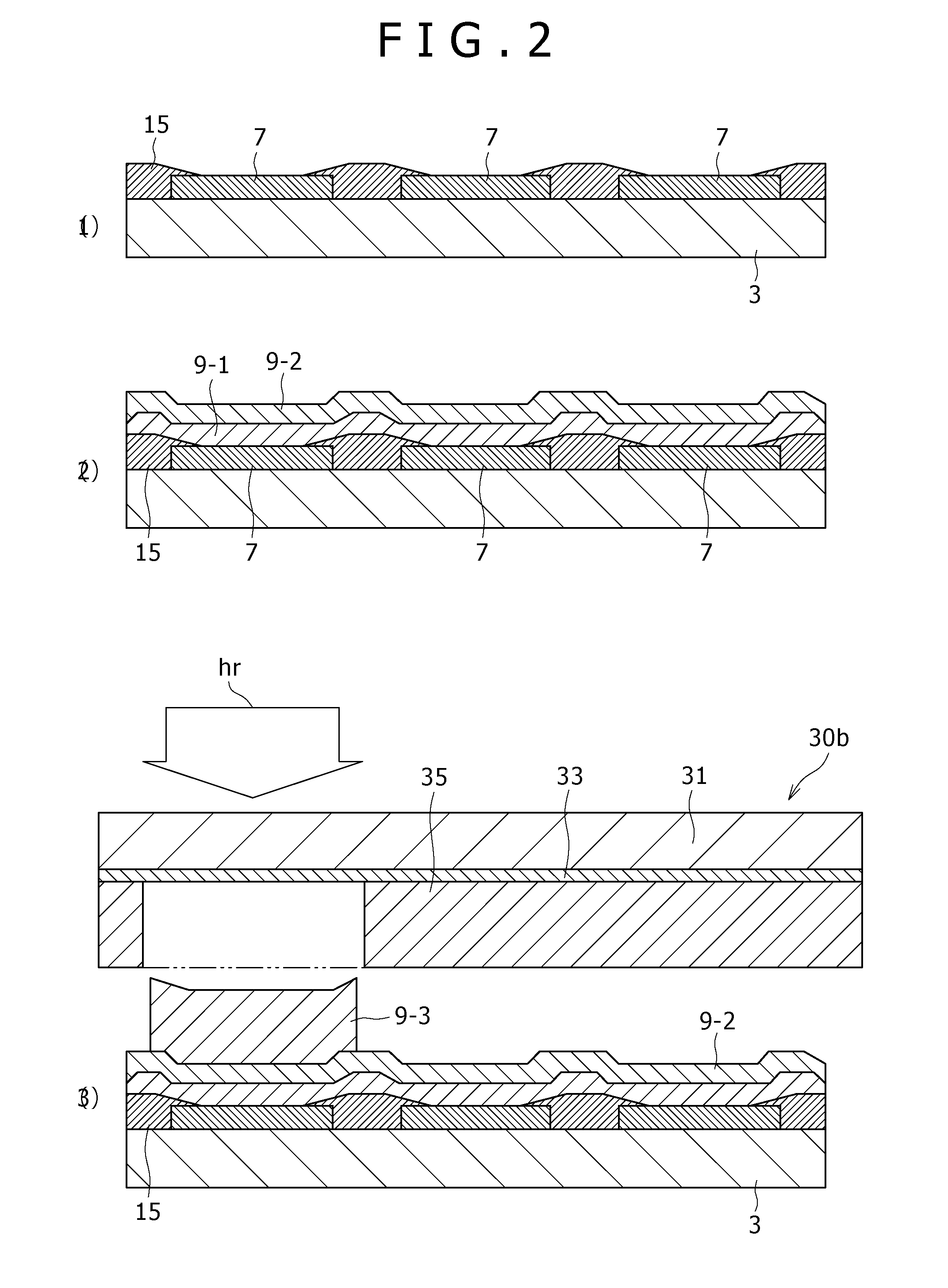
In addition, in general film deposition including laser transfer method, the larger a target film thickness is, the larger the error amount between the target film thickness and the film thickness actually deposited.

Method used


Image

  • Display and method for manufacturing display
  • Display and method for manufacturing display
  • Display and method for manufacturing display

Examples


working example

[0104]Ten blue light-emitting elements were fabricated of which micro resonator structure was designed to satisfy the first-order interference condition.

[0105]The chromaticity and light emission efficiency of the fabricated ten blue light-emitting elements were measured by using a spectral radiance meter with a constant current having a current density of 10 mA / cm2 applied to the blue light-emitting elements. Of the elements, an element from which intended light emission characteristics were obtained was defined as the design center. Furthermore, the sample with the largest film-thickness deviation in the positive direction was defined as Sample 1, while the sample with the largest film-thickness deviation in the negative direction was defined as Sample 2. The evaluation results are shown in Table 1.

TABLE 1Difference inLight EmissionLight EmissionEfficiency fromCIExCIEyEfficiency(cd / A)Design Center(%)Design0.1350.0692.611—CenterSample 10.1330.0742.8448.9Sample 20.1370.0642.322−11.1

[...


PUM


Abstract

Disclosed herein a display including: a plurality of organic electroluminescent elements configured to be arranged over a substrate and be each obtained by depositing a lower electrode, an organic layer including at least a light-emitting layer, and an upper electrode in that order, the organic layer of each of the organic electroluminescent elements being adjusted to have a film thickness that allows resonance of a wavelength of luminescent light generated in the light-emitting layer, wherein the film thickness of the organic layer in a first organic electroluminescent element that generates luminescent light having a shortest wavelength among the plurality of organic electroluminescent elements is set larger than the film thickness of the organic layer in a second organic electroluminescent element that generates luminescent light having a wavelength longer than the shortest wavelength of luminescent light generated in the first organic electroluminescent element.

Description

CROSS REFERENCES TO RELATED APPLICATIONS[0001]The present invention contains subject matter related to Japanese Patent Application JP 2006-198844, filed in the Japan Patent Office on Jul. 21, 2006, the entire contents of which being incorporated herein by reference.BACKGROUND OF THE INVENTION[0002]1. Field of the Invention[0003]The present invention relates to a display and a method for manufacturing the same, and particularly to a display including organic electroluminescent elements of plural colors and a method for manufacturing the same.[0004]2. Description of the Related Art[0005]In recent years, as an alternative to CRT displays, flat panel displays with a smaller weight and lower power consumption are being researched and developed. Among flat panel displays, displays using organic electroluminescent elements are self-luminous displays and have high response speed, and therefore are attracting attention as displays that can be driven with low power consumption.[0006]In order ...

Claims


Application Information

Patent Timeline
Patent Type & Authority Applications(United States)
IPC IPC(8): H01J1/62H01J9/02H01L51/54H01L51/56
CPCC09K11/06C09K2211/1007C09K2211/1011C09K2211/1014H05B33/10H01J1/74H01L27/3211H01L51/5265H01L2251/558C09K2211/1088H10K59/35H10K2102/351H10K59/876H05B33/14H05B33/22H10K50/852
Inventor MATSUDA, EISUKETAKAGI, RYOKO
Owner SONY CORP
Learn More