Silicide cap structure and process for reduced stress and improved gate sheet resistance

a silicide cap and cap structure technology, applied in the field of self-aligned metal silicide contact structure, can solve the problems of increasing resistance and restricting the thermal process window, and achieve the effect of reducing gate and source/drain sheet resistan

Inactive Publication Date: 2008-01-24
IBM CORP
View PDF13 Cites 10 Cited by
  • Summary
  • Abstract
  • Description
  • Claims
  • Application Information

AI Technical Summary

Benefits of technology

[0012] One object of the present invention is to provide a semiconductor structure and method of fabricating a semiconductor structure having reduced gate and source / drain sheet resistances.
[0013] Another object of the present invention is to provide an improved self-aligned silicide process (salicide process) for a semiconductor transistor or memory device structure exhibiting reduced gate and source / drain sheet resistance.
[0014] An additional object of the present invention is to provide maximum utilization of the metal deposited in S / D regions between narrowly spaced gates where the amount of metal deposited from the sputter source may be reduced by shielding from the gate structures.
[0016] Yet another object of the present invention is to provide an improved self-aligned silicide process (salicide process) that includes depositing a composite cap layer that exhibits a lower stress build-up and lower nitrogen penetration than in the conventional TiN cap process used in forming a semiconductor transistor or memory device structure.
[0017] Thus, according to the invention, such a composite cap structure is employed in a salicide process that includes a top layer providing a penetration barrier against oxygen, i.e., Ti or Co, and an intermediate layer adjacent to the silicide forming metal such as W or Mo that prevents the oxygen barrier from reacting with the silicide forming materials. The composite silicide cap provides a barrier to oxygen penetration into the metal used to form the silicide, and additionally has mechanical properties that allow selective formation of silicide on active areas, but not over insulators with out excessive mechanical energy build up within the cap and metal layer that leads to voiding and bridging of the silicide. That is, the provision of a thin W layer of about 5 nm thickness in the composite cap structure reduces the stress effects and high Young's modulus of this material (over TiN) and, with an additional counter layer of Co or Ti on top, reduces oxygen penetration and provide a counter tensile stress layer to reduce the mechanical energy of the composite stack.
[0022] an oxygen barrier layer atop the intermediate metal barrier layer, wherein, as a result of an applied anneal to the structure, a silicide region is formed that exhibits improved sheet resistance.

Problems solved by technology

However, even rapid thermal annealing (RTA) can lead to agglomeration and increased resistance.
This restricts the thermal process window for the reaction of the metal films to form low resistance contacts before the films become unstable.
Attempts to implement a W sputter deposited cap in the past have been plagued by voids in the silicide and bridging, leaving only a small temperature and thickness window in which it would work.

Method used


Image

  • Silicide cap structure and process for reduced stress and improved gate sheet resistance
  • Silicide cap structure and process for reduced stress and improved gate sheet resistance
  • Silicide cap structure and process for reduced stress and improved gate sheet resistance

Examples


Embodiment Construction

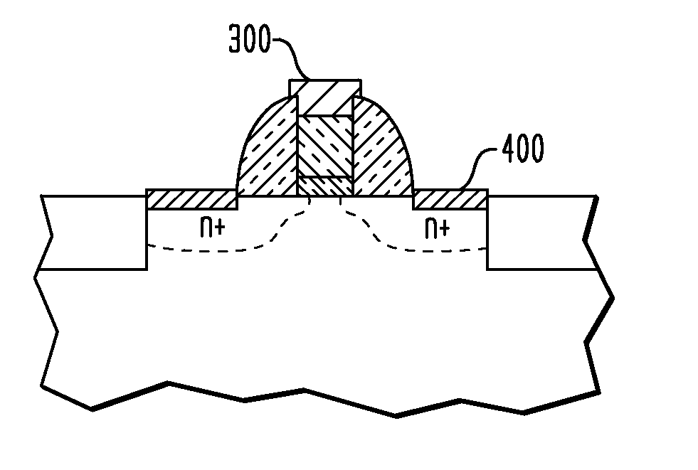
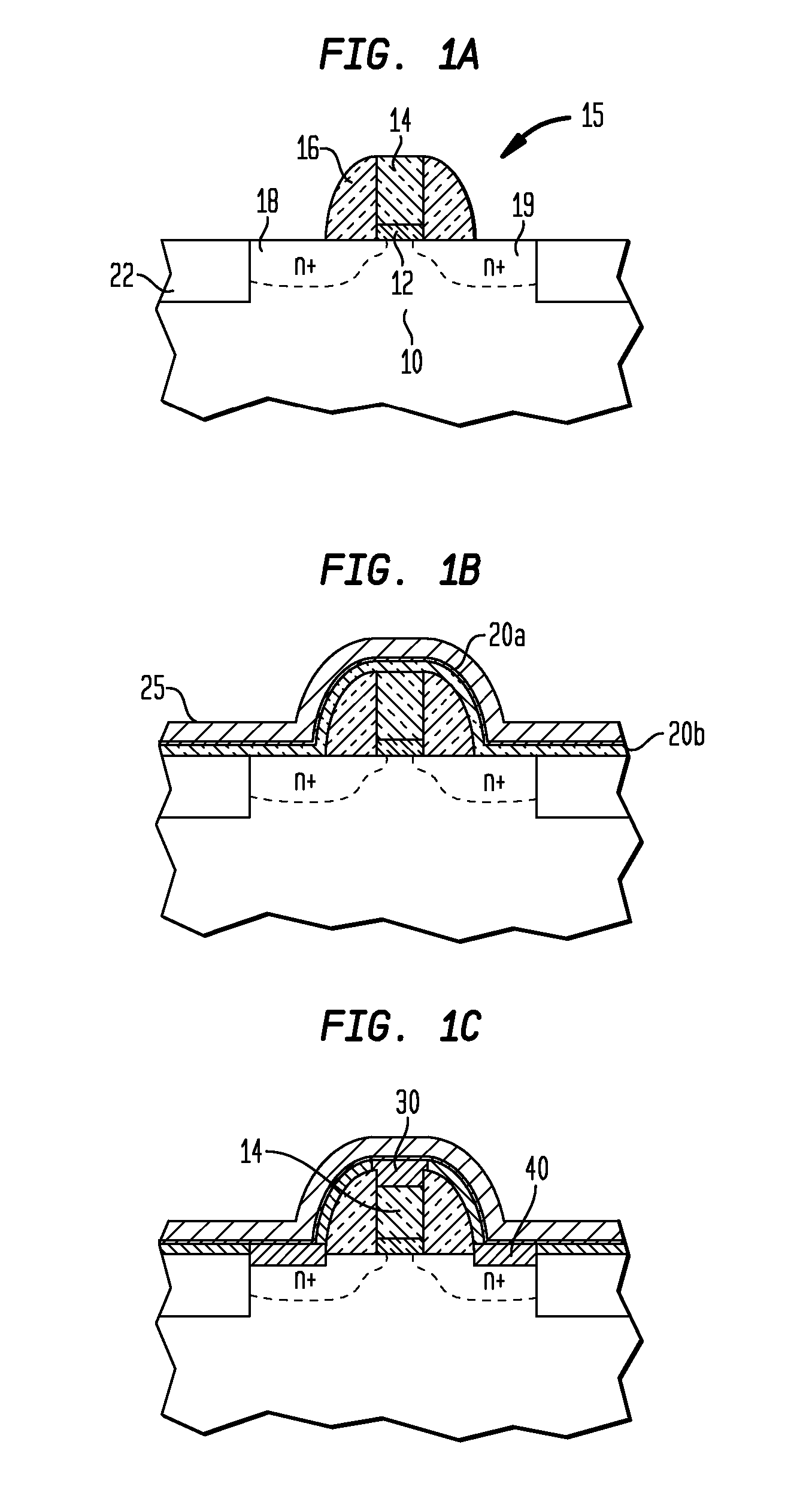
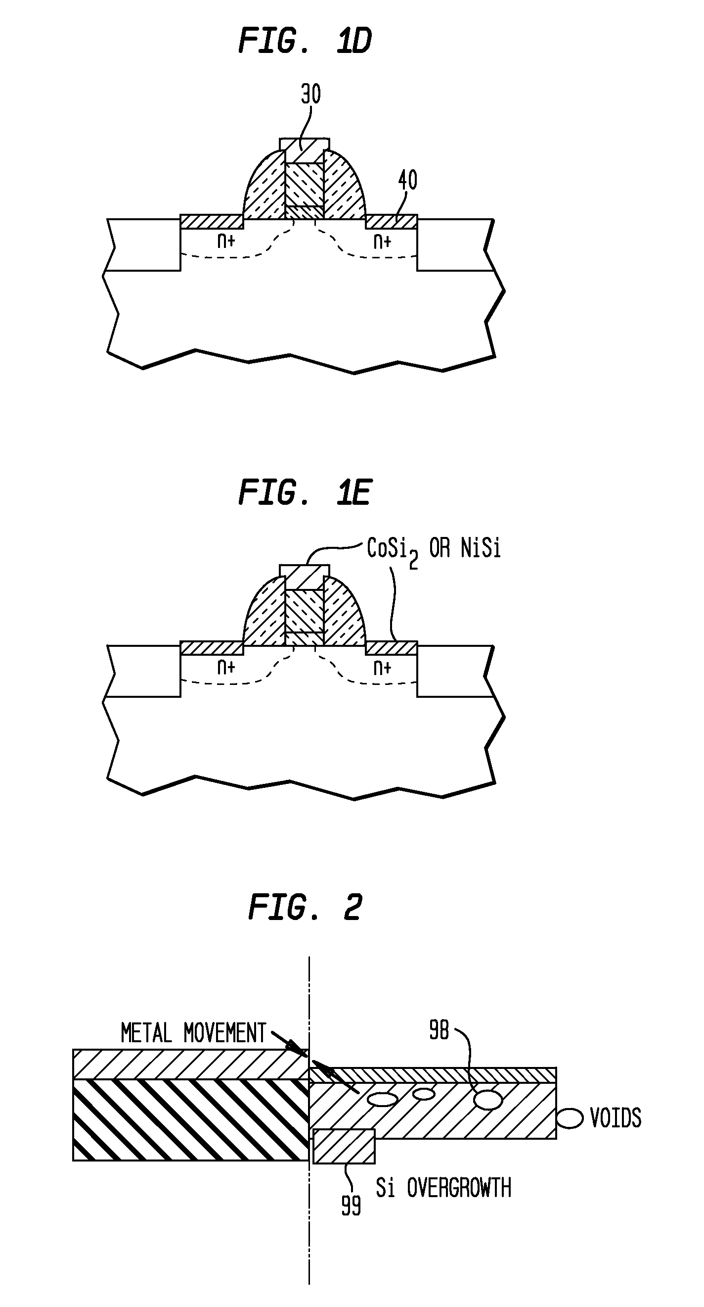
[0041] The present invention, which provides a method of fabricating a semiconductor transistor device structure having a silicide region formed atop the transistor source / drain regions and formed atop the transistor gate region, will now be described in greater detail.

[0042] According to the invention, a composite silicide cap structure resulting from a salicide process includes a top layer of material providing a penetration barrier against oxygen, e.g., Ti or Co, and an intermediate layer of material adjacent to the silicide forming metal such as W, or molybdenum (Mo) that prevents the oxygen barrier from reacting with the silicide forming materials. The silicide cap provides a barrier to oxygen penetration into the metal used to form the silicide, and additionally has mechanical properties that allow selective formation of silicide on active areas, but not over insulators with out excessive mechanical energy build up within the cap and metal layer that leads to voiding and brid...


PUM

PropertyMeasurementUnit
thicknessaaaaaaaaaa
thicknessaaaaaaaaaa
thicknessaaaaaaaaaa

Abstract

A silicide cap structure and method of fabricating a silicide cap having a low sheet resistance. The method provides a semiconductor substrate and a MOSFET structure comprising a gate insulator on the substrate, an Si-containing gate electrode on the gate insulator layer, and source / drain diffusions. Atop the gate electrode and source / drain diffusions is formed a layer of metal used in forming a silicide region atop the transistor gate electrode and diffusions; an intermediate metal barrier layer formed atop the silicide forming metal layer; and, an oxygen barrier layer formed atop the intermediate metal barrier layer. As a result of annealing the MOSFET structure, resulting formed silicide regions exhibit a lower sheet resistance. As the intermediate metal barrier layer comprises a material exhibiting tensile stress, the oxygen barrier layer may comprise a compressive material for minimizing a total mechanical stress of the cap structure and underlying layers during the applied anneal.

Description

CROSS-REFERENCE TO RELATED APPLICATIONS [0001] This application is a divisional of U.S. application Ser. No. 10 / 905,949, filed Jan. 27, 2005, which relates to commonly-owned, co-pending U.S. patent application Ser. No. 10 / 709,534, filed May 12, 2004 entitled “Method For Controlling Voiding and Bridging in Silicide Formation” the whole contents and disclosure of which are incorporated by reference as if fully set forth herein.FIELD OF THE INVENTION [0002] The present invention relates to semiconductor device manufacturing, and more particularly to a self-aligned metal silicide contact structure that exhibits lower sheet resistance and, a method of manufacture. The present invention is also related to complementary metal oxide semiconductor (CMOS) structures which include the self-aligned silicide contacts. BACKGROUND OF THE INVENTION [0003] A key to continued CMOS miniaturization is the ability to scale down the horizontal and vertical dimensions of the semiconductor device while inc...

Claims


Application Information

Patent Timeline
Patent Type & Authority Applications(United States)
IPC IPC(8): H01L21/336H01L21/44
CPCH01L21/28052H01L29/665H01L21/28518H01L21/28114
Inventor GULARI, LEVENTMELLO, KEVIN E.PURTELL, ROBERT J.WANG, YUN-YUWONG, KEITH K.
Owner IBM CORP
Why Eureka
Try Eureka