
Methods and systems for selectively depositing si-containing films using chloropolysilanes

a technology of chloropolysilane and selective depositing, which is applied in the direction of polycrystalline material growth, crystal growth process, chemically reactive gas, etc., can solve the problems of few advantages, few studies performed, and the development of commercial sources of trisilanes in the past , to achieve the effect of less sensitiv

Inactive Publication Date: 2008-01-31
ASM AMERICA INC
View PDF4 Cites 70 Cited by
  • Summary
  • Abstract
  • Description
  • Claims
  • Application Information

AI Technical Summary

Benefits of technology

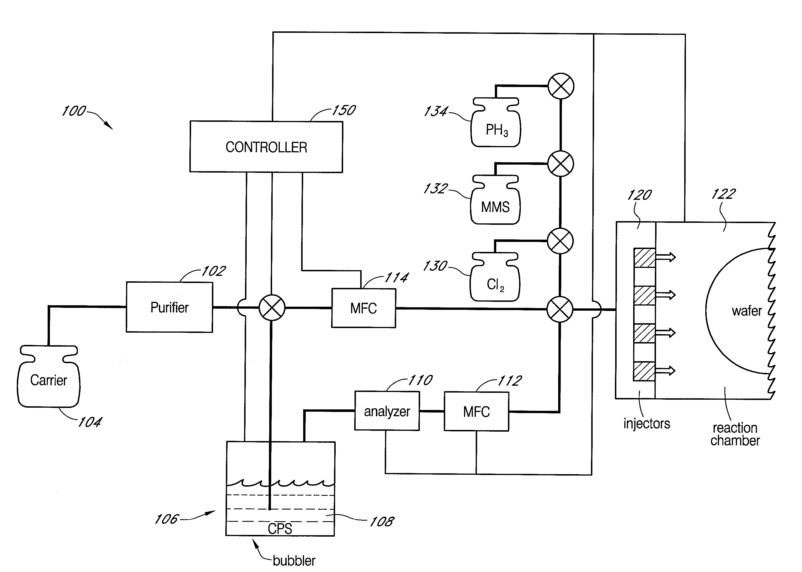
[0012] Deposition processes have now been discovered that utilize chloropolysilanes as Si precursors. In embodiments, these depositions are less sensitive to nucleation phenomena compared to disilane or trisilane, and thus are particularly well-suited for providing selectivity to the deposition process. The processes work well with additive process gases, including carbon, germanium and / or dopant sources, and thus are useful for making various Si-containing films and for incorporating strain into the deposited layer or adjacent structures. In embodiments, the deposition processes employ a chlorine gas in combination with selected chloropolysilanes, particularly monochlorodisilane, dichlorodisilane, trichlorodisilane, and / or tetrachlorodisilane. Other embodiments provide systems useful for employing the chloropolysilanes to selectively deposit Si-containing films.
[0015] selectively depositing a Si-containing film onto a single crystal surface region of a substrate disposed within the CVD chamber under the selective CVD condition while minimizing deposition onto a non-single crystalline surface region of the substrate during the selective deposition.

Problems solved by technology

While trisilane has long been known as a theoretical precursor for the deposition of silicon, few studies have been performed on it and few advantages have been recognized.
Accordingly, significant commercial sources of trisilane have not developed historically.

Method used


Image

  • Methods and systems for selectively depositing si-containing films using chloropolysilanes
  • Methods and systems for selectively depositing si-containing films using chloropolysilanes
  • Methods and systems for selectively depositing si-containing films using chloropolysilanes

Examples


example 1

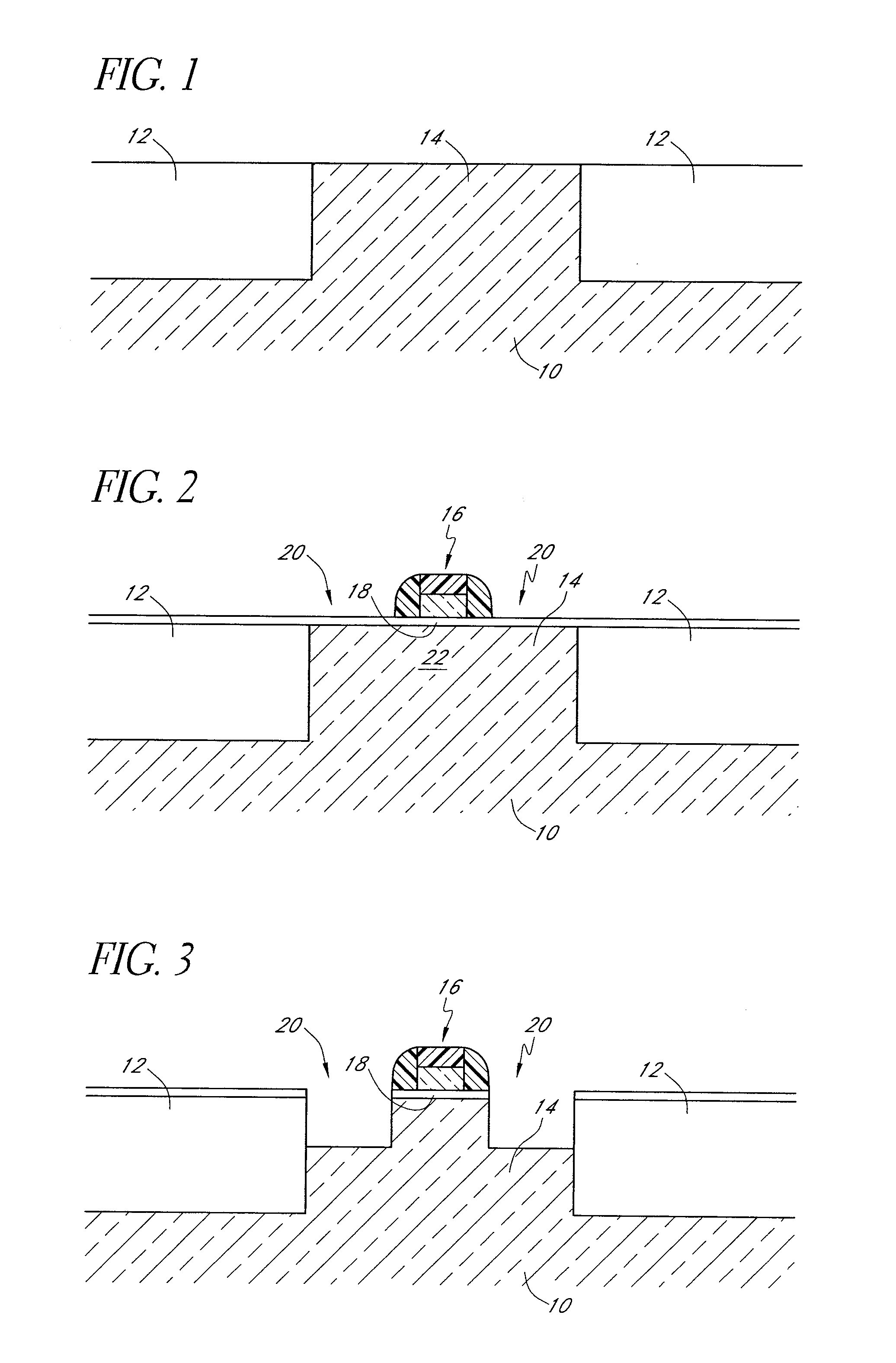
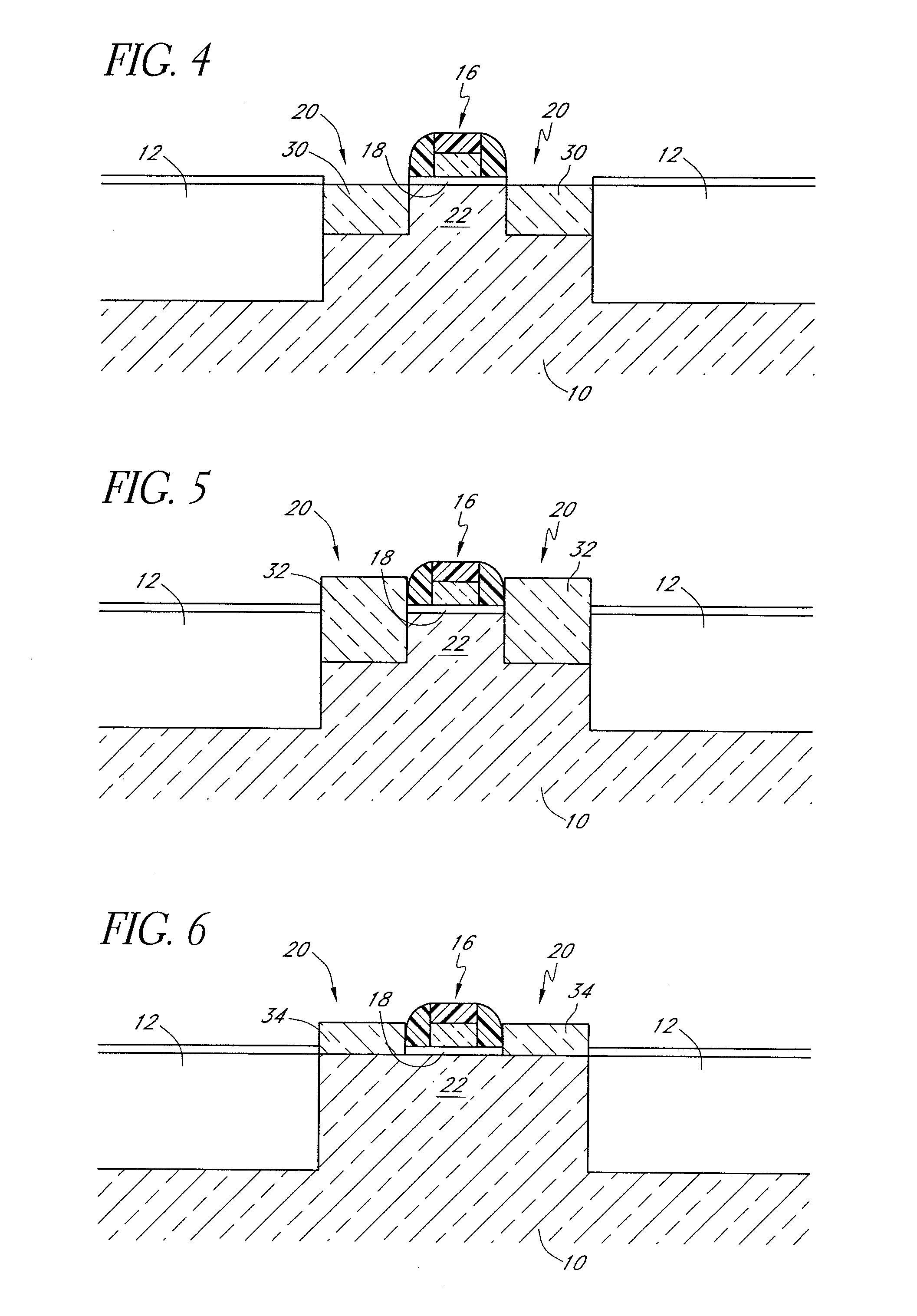
[0109] This example illustrates the deposition of selective epitaxial silicon films over mixed morphology substrates.

[0110] An eight-inch unpatterned Si wafer substrate and separate wafer with a fully oxidized (1000′) surface are serially loaded into and processed in an Epsilon E2500™ reactor system. The substrates are each introduced into the reactor system at 900° C., a hydrogen flow rate of 20 slm is used initially for the bare wafer, and the substrate is allowed to stabilize for 1 minute. The hydrogen flow is then shut down as the temperature of the substrate is reduced to 550° C. The substrate is then allowed to stabilize for 10 seconds, after which time a flow of 20 standard cubic centimeters per minute (sccm) of chloropolysilane (a mixture consisting essentially of 75% by weight dichlorodisilane and 25% by weight trichlorodisilane) and a flow of 12.5 sccm of chlorine is introduced at a deposition pressure of 64 Torr for about 3 minutes. A continuous, uniform silicon film hav...

example 2

[0111] Deposition conditions are varied to identify a selective CVD condition as follows: A quartz tube furnace is heated to temperature of about 550° C. A flow of 20 sccm of chloropolysilane (a mixture consisting essentially of 75% by weight dichlorodisilane and 25% by weight trichlorodisilane) and a flow of 75 sccm of chlorine is introduced to the quartz tube furnace in the absence of a carrier gas at a deposition pressure of 64 Torr. No deposition is observed. Since the furnace is quartz, deposition on the walls is indicative of CVD conditions on an oxide surface, and thus it is apparent that this is likely to be an etching condition for oxide surfaces. The chlorine flow is reduced in stages to about 12.5 sccm over the course of about 5-6 minutes, at which time a deposit (silicon) forms on the walls of the furnace, indicating that deposition is less selective than at higher chlorine flow rates. Thus, under these conditions, this CVD condition is likely to be selective on a mixed ...

example 3

[0112] Deposition conditions are varied to identify a selective CVD condition as described in EXAMPLE 2, except that the deposition temperature is 500° C., the deposition pressure is 4 Torr, and a 300 sccm helium carrier gas is used. As in EXAMPLE 2, the chloropolysilane flow is 20 sccm and the initial chlorine flow rate is 75 sccm. At this initial condition, no deposition is observed, and thus it is apparent that this is likely to be an etching condition for oxide surfaces. The chlorine flow is reduced in stages to about 20 sccm, at which time a slight deposit (silicon) begins to form on the walls of the furnace, indicating that deposition is less selective than at higher chlorine flow rates. Thus, under these conditions, this CVD condition is likely to be selective on a mixed substrate at a chlorine flow slightly higher than about 20 sccm. The deposition becomes progressively heavier as the chlorine flow is reduced in stages to about 2.5 sccm, then progressively lighter as the chl...


PUM

PropertyMeasurementUnit
temperatureaaaaaaaaaa
pressureaaaaaaaaaa
temperatureaaaaaaaaaa

Abstract

Chloropolysilanes are utilized in methods and systems for selectively depositing thin films useful for the fabrication of various devices such as microelectronic and / or microelectromechanical systems (MEMS).

Description

[0001] This application claims priority to U.S. Provisional Patent Application Ser. No. 60 / 809,745, filed May 31, 2006, which is hereby incorporated by reference in its entirety.BACKGROUND OF THE INVENTION [0002] 1. Field of the Invention [0003] This invention relates to systems and methods for using chlorinated disilanes and trisilanes to selectively deposit Si-containing films useful for the fabrication of various devices such as microelectronic and / or microelectromechanical systems (MEMS). [0004] 2. Description of the Related Art [0005] A variety of methods are used in the semiconductor manufacturing industry to deposit materials onto surfaces. For example, one of the most widely used methods is chemical vapor deposition (“CVD”), in which atoms or molecules contained in a vapor deposit on a surface and build up to form a film. Deposition of silicon-containing (“Si-containing”) materials using conventional silicon sources and deposition methods, particularly non-epitaxial depositi...

Claims


Application Information

Patent Timeline
Patent Type & Authority Applications(United States)
IPC IPC(8): C23C16/00
CPCC23C16/04C23C16/24C30B25/02C30B25/18C30B29/06H01L21/02381H01L21/28518H01L21/02532H01L21/02576H01L21/02579H01L21/0262H01L21/02639H01L21/02529
Inventor TOMASINI, PIERREARENA, CHANTALBAUER, MATTHIASCODY, NYLESBERTRAM, RONALDWEN, JIANQINGSTEPHENS, MATTHEW D.
Owner ASM AMERICA INC
Learn More