

Semiconductor device and manufacturing method thereof
a technology of semiconductor devices and manufacturing methods, applied in the direction of semiconductor devices, basic electric elements, electrical appliances, etc., can solve the problems of difficult to improve the channel mobility, and achieve the effect of reducing the resistance in the channel region
- Summary
- Abstract
- Description
- Claims
- Application Information
AI Technical Summary
Benefits of technology
Problems solved by technology
Method used
Image

Examples
first embodiment
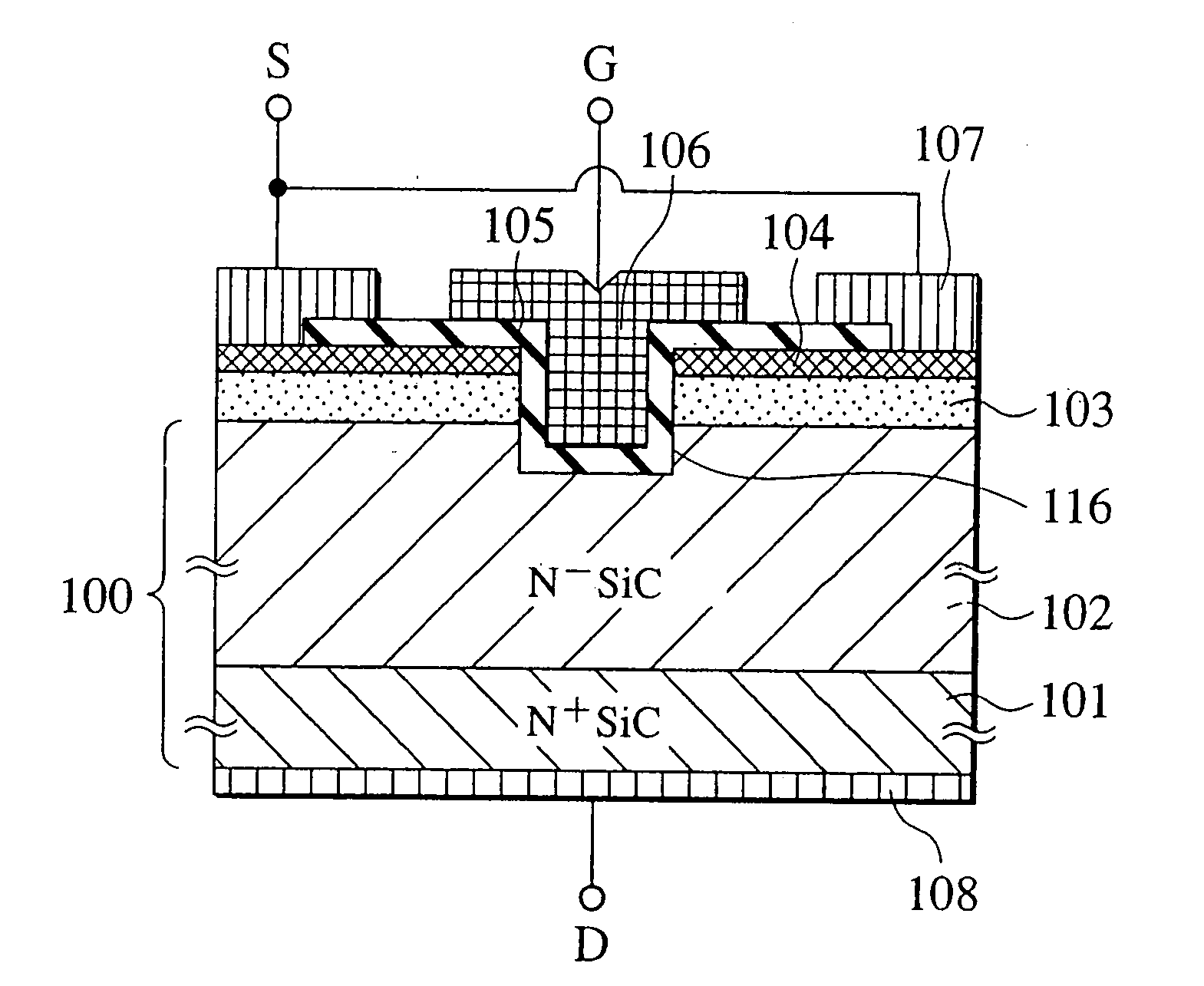
[0049]FIG. 1 shows a semiconductor device of the first embodiment according to the present invention. The figure is a cross sectional view of two cells as structural units which face each other. A description will be provided for this embodiment, citing an example of a semiconductor device which uses silicon carbide as a material of the substrate.
[0050] For example, an n− type drain region 102 is formed on an n+ type substrate region 101 which is made up of silicon carbide whose polytype is 4H. In addition, a source region 103 which is made up of, for example, n− type polycrystalline silicon is formed on a main interface that is situated on the opposite side of the drain region 102 in relation to a junction interface between the drain region 102 and the substrate region 101. In other words, the contact between the drain region 102 and the source region 103 is formed of heterojunction which is made up of silicon carbide and polycrystalline silicon whose bandgaps are different from e...
second embodiment
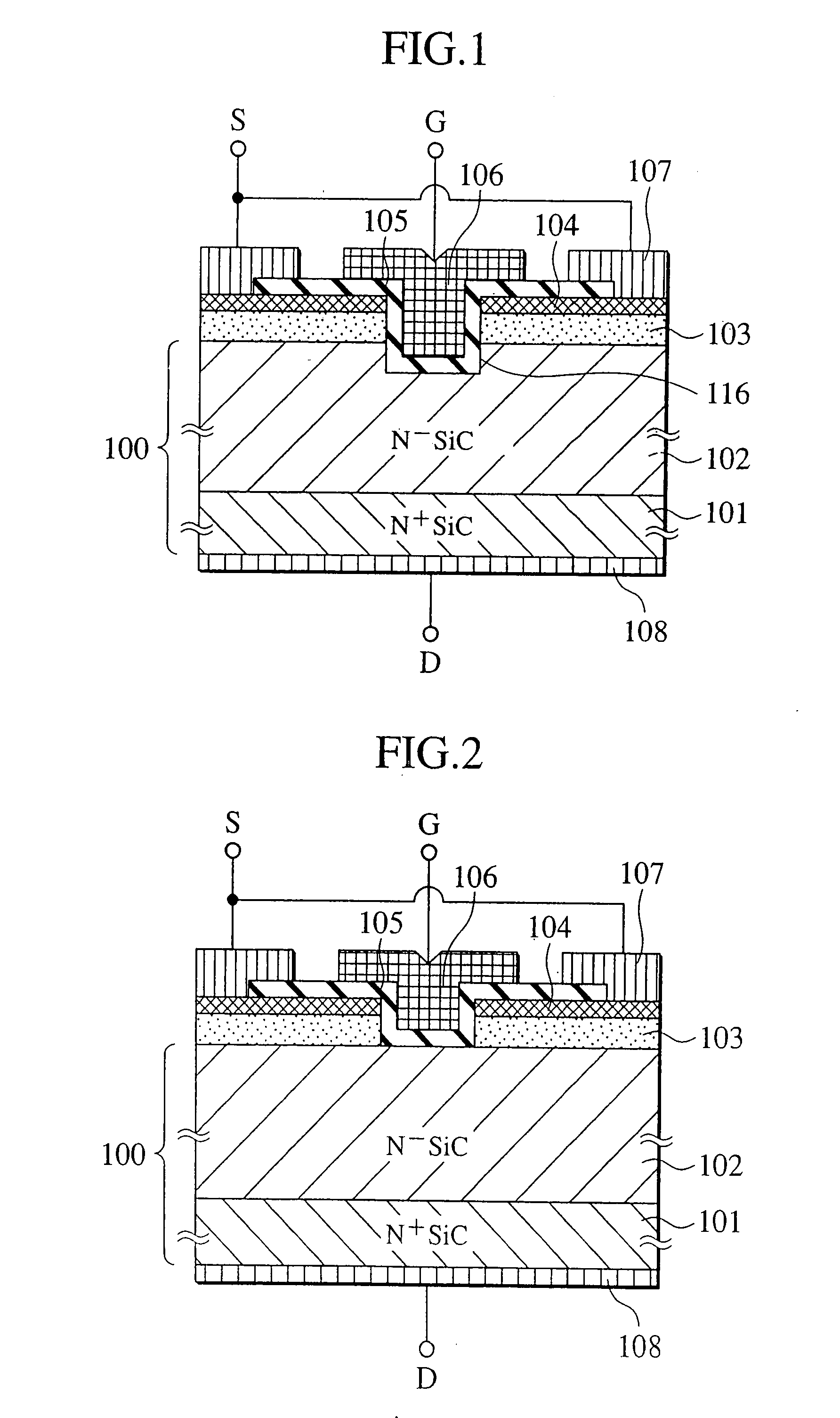
[0079]FIG. 10 shows a semiconductor device according to a second embodiment of the present invention. FIG. 10 is a cross sectional view corresponding to FIG. 1 of the first embodiment. For this second embodiment, descriptions of operations which are the same as operations which are performed as shown in FIG. 1 will be omitted, and detailed descriptions will be provided for features which are different from those which have been described in FIG. 1.
[0080] Features of the second embodiment are as shown in FIG. 10. A semiconductor device according to the second embodiment includes a withstanding voltage region 109 which is a second hetero-semiconductor region which is in contact with the semiconductor body and the source region 103 which is the first hetero-semiconductor region, and whose bandgap is different from that of the semiconductor body. Junction between the withstanding voltage region 109 and the semiconductor substrate is so formed that voltage withstanding in the portion of...
third embodiment
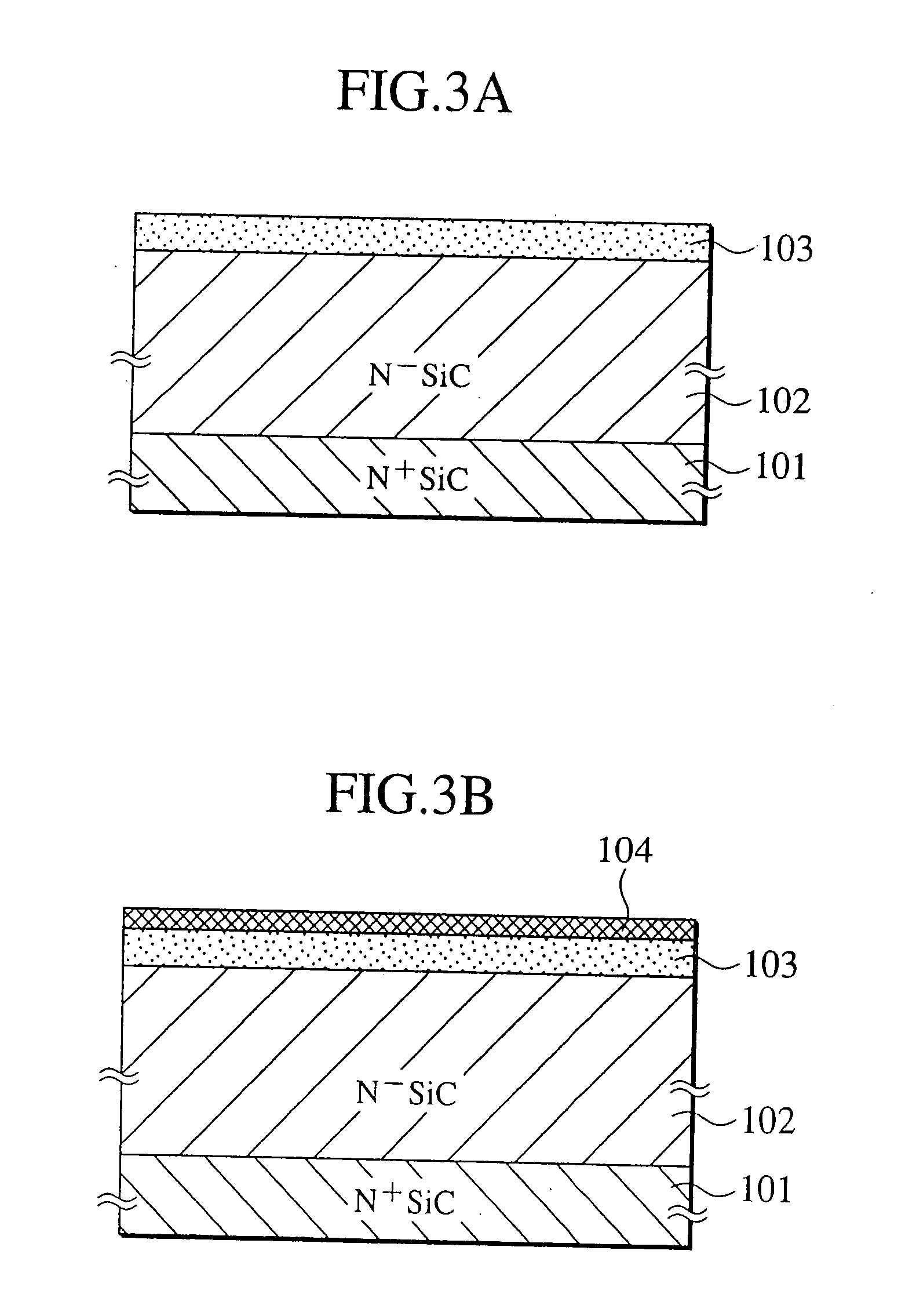
[0083]FIG. 11 shows a semiconductor device according to a third embodiment of the present invention. FIG. 11 is a cross sectional view corresponding to FIG. 10 of the second embodiment. For this third embodiment, descriptions of operations which are the same as operations which are performed as shown in FIG. 10 will be omitted, and detailed descriptions will be provided for features which are different from those which have been described in FIG. 10.
[0084] According to this third embodiment, as shown in FIG. 11, the source region 103 is formed of an n+ type whose properties include high conductivity, and the low resistance region 104 is formed of n+ type polycrystalline silicon which is the same material used for the source region 103 instead of, for example, cobalt silicide which has been used, as shown in FIG. 10, for the low resistance region 104. These constructions enable manufacturing processes to be simplified. In addition, an interlayer dielectric 110 is formed between the ...
PUM
 Abstract
Description
Claims
Application Information