Eureka AIR delivers breakthrough ideas for toughest innovation challenges, trusted by R&D personnel around the world.

Organic Material For Ferroelectric Semiconductor Device

a technology of ferroelectric semiconductors and organic materials, which is applied in the field of organic materials for ferroelectric semiconductor devices, can solve the problems of inorganic ferroelectrics, polarization characteristics may be deteriorated, and non-volatile memory devices that can maintain data stored therein without a separate power supply have attracted attention

Inactive Publication Date: 2008-01-31
UNIV OF SEOUL FOUND OF IND - ACADEMIC
View PDF3 Cites 2 Cited by
  • Summary
  • Abstract
  • Description
  • Claims
  • Application Information

AI Technical Summary

Benefits of technology

[0006] The present invention has been contrived taking the above-described circumstances into consideration and, an object of the present invention is to provide an environment-friendly and low cost organic material having excellent ferroelectric characteristics for semiconductor device.

Problems solved by technology

However, non-volatile memory devices that can maintain data stored therein without a separate power supply have attracted attention recently.
However, such inorganic ferroelectrics have some drawbacks in that they are very expensive; the polarization characteristics may be deteriorated according to the lapse of time; the formation of thin films requires a high temperature treatment; and various expensive equipments are needed in using the inorganic ferroelectrics.

Method used


Image

  • Organic Material For Ferroelectric Semiconductor Device
  • Organic Material For Ferroelectric Semiconductor Device
  • Organic Material For Ferroelectric Semiconductor Device

Examples


Embodiment Construction

[0016] Hereinafter, the present invention will now be described more fully with reference to the accompanying drawings, in which preferred embodiments of the invention are shown. This invention may, however, be embodied in different forms and should not be construed as limited to the embodiments set forth herein. Rather, these embodiments are provided so that this disclosure will be thorough and complete, and will fully convey the scope of the invention to those skilled in the art.

[0017] First, the basic concept of the present invention will now be described.

[0018] At present, various kinds of organic materials having ferroelectric characteristics have been known. The typical organic materials may be exemplified by polyvinylidene fluoride (PVDF), PVDF polymer, PVDF copolymer or PVDF terpolymer and, further, odd-numbered nylon, cyano-polymer and their polymer or copolymer. Among such ferroelectric organic materials described above, PVDF, its polymer, copolymer and terpolymer have b...


PUM

PropertyMeasurementUnit
temperatureaaaaaaaaaa
thicknessaaaaaaaaaa

Abstract

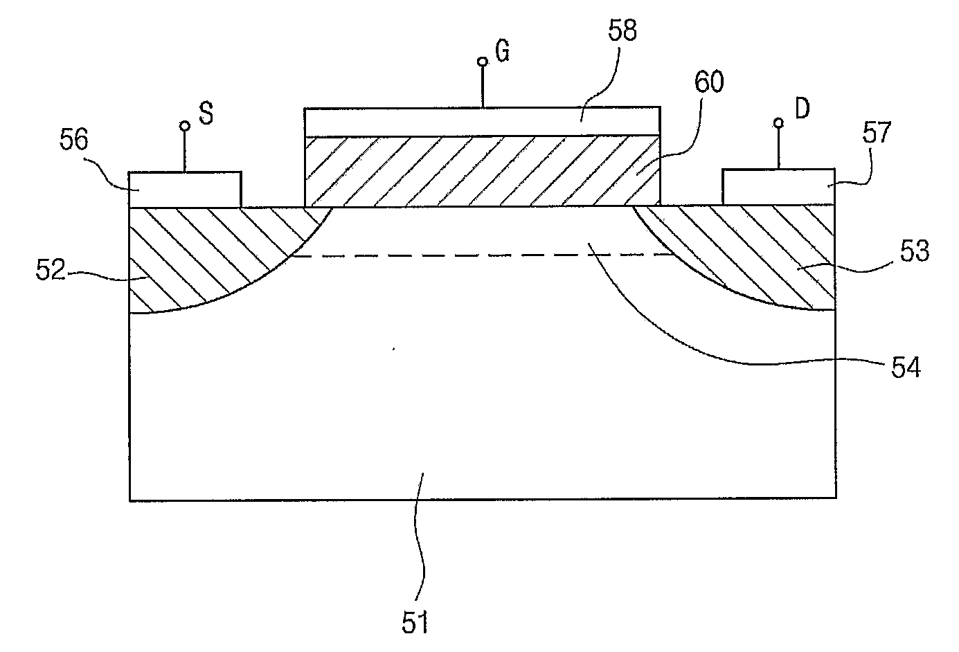
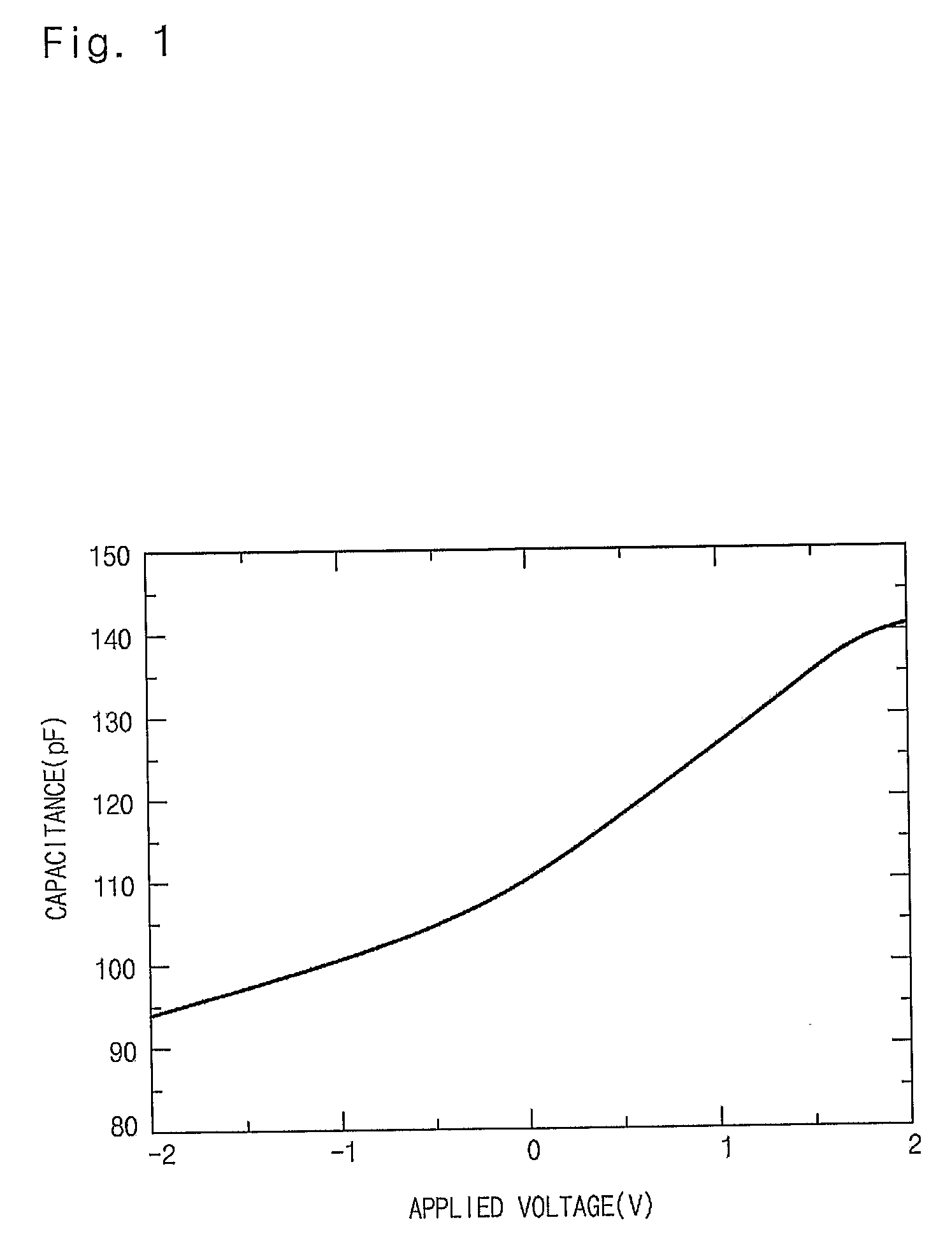
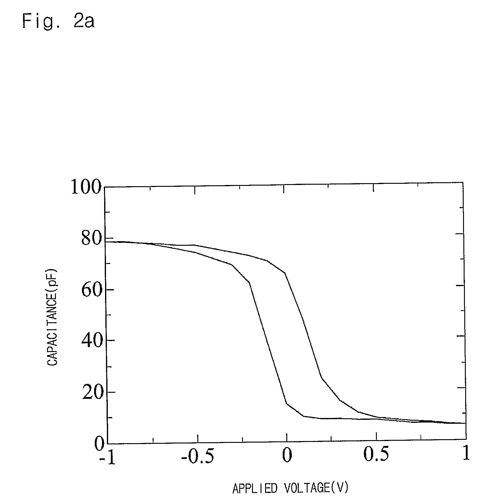
Disclosed relates to an organic material for a ferroelectric semiconductor device, which can be effectively used as a dielectric material of the ferroelectric semiconductor device, such as PVDF, etc. The PVDF having four crystal structures of α, β, γ, and δ shows a good hysteresis characteristic in the crystal structure of β-phase. A PVDF thin film having a crystal structure of β-phase has excellent hysteresis characteristics that show a capacitance value is decreased with the increase of an applied voltage in about 0 to 1V and increased with the decrease of an applied voltage in about 0 to −1V. A ferroelectric organic material having a crystal structure of β-phase is used on a channel region (54) between source and drain regions (52 and 53) of a silicon substrate (51). As ferroelectric organic materials, polyvinylidene fluoride (PVDF), PVDF polymer, PVDF copolymer or PVDF terpolymer and, further, odd-numbered nylon, cyano-polymer and their polymer or copolymer, etc. may be used.

Description

TECHNICAL FIELD [0001] The present invention relates to a ferroelectric semiconductor device and, more particularly, to an organic material for a ferroelectric semiconductor device that can be effectively used as a dielectric material for the ferroelectric semiconductor device. BACKGROUND ART [0002] At present, memory devices have been necessarily applied to most electronic apparatus including personal computers. Such memory devices may be classified roughly into ROMs, such as electrically programmable read only memory (EPROM), electrically erasable PROM (EEPROM), flash ROM, etc., and RAMs, such as static random access memory (SRAM), dynamic RAM (DRAM), ferroelectric RAM (FRAM), etc. The memory device is fabricated generally by arranging capacitors and transistors on a semiconductor wafer. [0003] In the conventional memory devices, various researches aimed mainly at increasing the density of memory cells have been made. However, non-volatile memory devices that can maintain data sto...

Claims


Application Information

Patent Timeline
Patent Type & Authority Applications(United States)
IPC IPC(8): C08F14/22
CPCC08F14/22G11B9/02G11C11/22C08F2/00C08F10/00
Inventor PARK, BYUNG-EUN
Owner UNIV OF SEOUL FOUND OF IND - ACADEMIC
Why Eureka
Eureka Blog
Learn More