

Method for the Contact Separation of Electrically-Conducting Layers on the Back Contacts of Solar Cells and Corresponding Solar Cells
a technology of solar cells and electrically-conducting layers, which is applied in the direction of photovoltaic energy generation, electrical apparatus, basic electric elements, etc., can solve the problems of reducing the efficiency of the solar cell, requiring a plurality of aligning masking steps, and therefore elaborate conventional so-called back-contact solar cells, etc., and achieves the effect of easy production
Inactive Publication Date: 2008-02-14
INST FUR SOLARENERGIEFORSCHUNG
View PDF19 Cites 144 Cited by
- Summary
- Abstract
- Description
- Claims
- Application Information
AI Technical Summary
Benefits of technology
[0013] There may be a need for the present invention to avoid or at least reduce the aforesaid problems and to provide a solar cell and a method of fabrication for a solar cell which achieves a high-efficiency and is easy to produce.
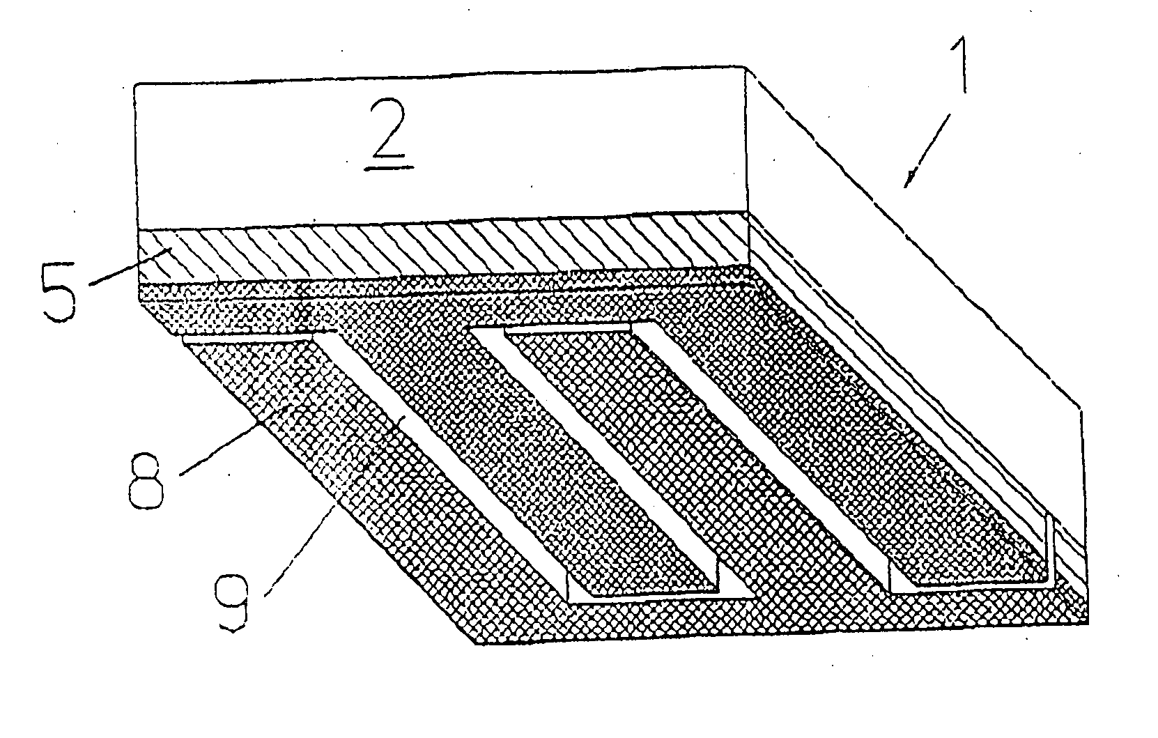
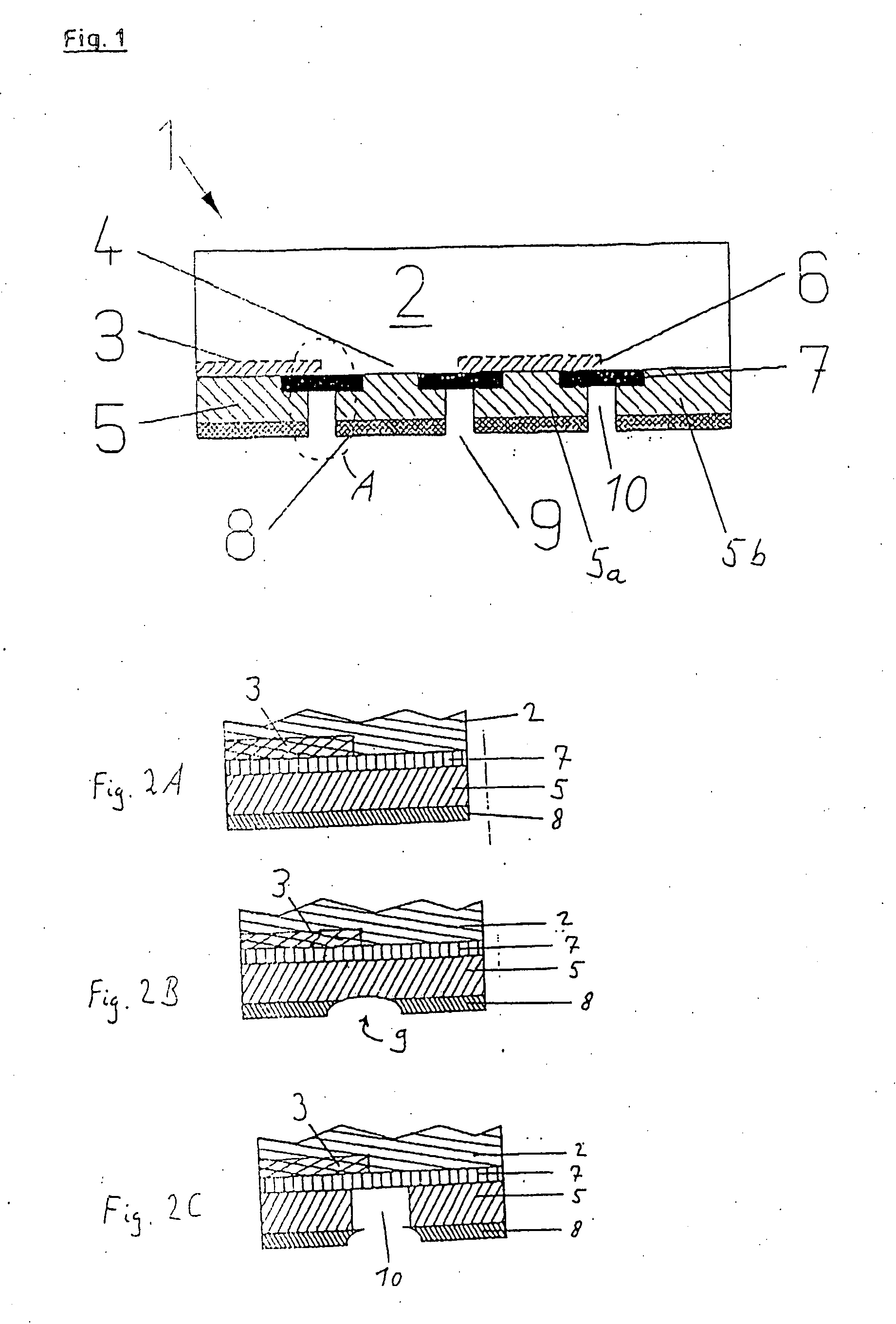
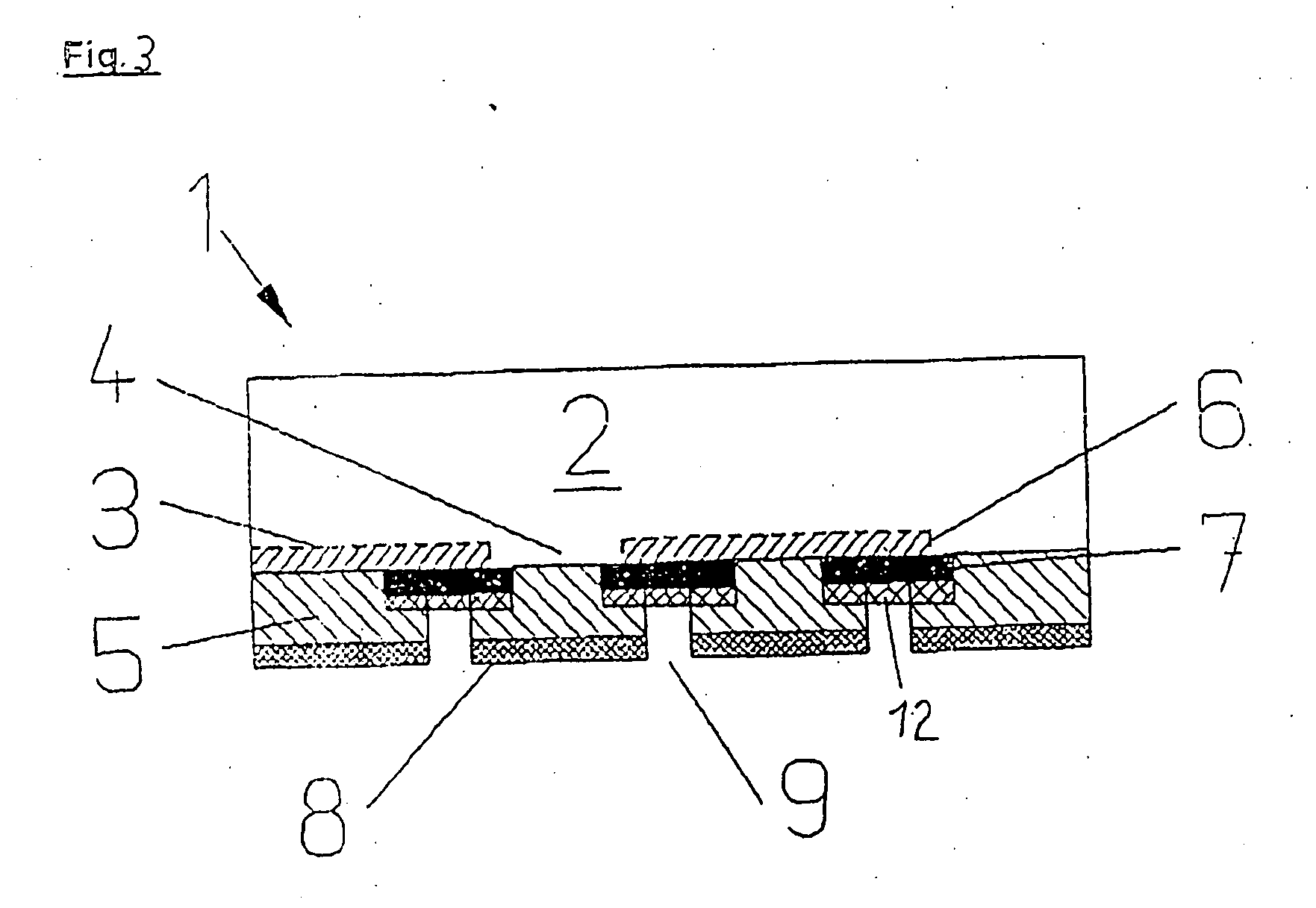
[0019] The emitter region to be formed subsequently and the base region of the solar cell have different n-type or p-type dopings. The definition of the two regions can be effected, for example, by locally protecting the base layer from diffusion using a masking layer or by diffusion over the entire surface and subsequently locally etching away the resulting emitter or removing it by means of laser ablation. The two regions can be nested in one another in a comb-like fashion (“interdigitated”). This has the result that charge carrier pairs generated in the semiconductor substrate only have to travel short distances up to a pn junction and are then separated there and can be removed via the metallisations contacting the respective regions. Recombination and series resistance losses can thus be minimised. In this case, the emitter region and the base region do not need to occupy the same surface fractions on the entire back-side surface.
[0021] The electrically insulating layer can be a dielectric which surface passivates both the substrate surface located thereunder and in particular the exposed pn-junction and also prevents short circuits between the emitter region and the base region caused by a metal layer subsequently located thereover.
[0038] The method according to the invention can achieve electrical insulation of the base contact from the emitter contact also located on the back side of the substrate in a simple manner. In this context, it is advantageous that the electrically insulating layer must cover the region boundary at all points but can also extend over substantially further regions of the substrate back side. A dielectric acting as an insulating layer can surface-passivate broad areas of the back surface of the substrate and must only be locally opened for contacting the emitter. The base contacts can be driven through the dielectric into the base region by an LFC method (laser fired contacts). Alternatively, the dielectric can be selectively locally opened prior to the metal deposition in the base region.
[0039] The local removal of the etch barrier layer must again lie merely somewhere in the area of the underlying junction regions and take place such that after the etching step, the entire base contact is completely electrically separated from the emitter contact. This means that the separating trenches insulating the emitter contact from the base contact should always run in regions in which the adjoining metal layers are insulated from the substrate back side by the underlying insulating layer. If broad areas of the substrate back side are covered by the insulating layer, this therefore provides great freedom with regard to the geometrical profile of the separating trench. It need not be aligned precisely above the region boundary of the surface-pn-junctions but can run laterally spaced apart from this region boundary. For example, the separating trench can be formed as meander-shaped. It can also be formed in such a manner that elongated metallisation finger regions insulated from one another by the separating trench taper from one side edge of the solar cell towards an opposite side edge.
[0043] In a further embodiment, another thin metal layer is located above the metal layer forming the contacts, this thin layer serving as an etch barrier layer during the fabrication of the solar cell. This layer is preferably formed using a solderable material such as, for example, silver or copper. The contacts whose metal layer can be made of difficult-to-solder aluminium can be easily soldered with the aid of this layer and the solar cells thus interconnected to one another.
Problems solved by technology
However, conventional so-called back-contact solar cells have several disadvantages.
Furthermore, conventional back-contact solar cells frequently suffer from local short circuits, caused for example by inversion layers between the base and the emitter region or by inadequate electrical insulation between the emitter and the base contact, leading to a reduced efficiency of the solar cell.
A disadvantage here is these methods require a plurality of aligning masking steps and are therefore elaborate.
In addition, the formation of elevated and recessed regions requires additional work steps compared to a solar cell with flat surfaces.
However, the efficiency of this cell is low since the inversion layer connects two contact systems which brings about a low parallel resistance and therefore a low fill factor.
In addition, the fabrication of a local emitter is technologically demanding in this cell.
A particular difficulty with back-contacted solar cells is the elaborate fabrication of the back side contacts where electrical short circuits must be absolutely avoided.
Method used
View moreImage
Smart ImageViewing Examples

Examples
first embodiment
[0045]FIG. 1 shows a schematic sectional view of a solar cell according to the invention according to a
[0046]FIG. 2A to 2C schematically illustrate process steps of a process sequence according to the invention.
second embodiment
[0047]FIG. 3 shows a schematic sectional view of a solar cell according to the invention with separating trenches which are laterally offset with respect to a region boundary.
third embodiment
[0048]FIG. 4 shows a schematic view of a solar cell according to the invention in which the separating trench has a meander-shaped configuration.
Login to View More PUM
 Abstract
A method for fabricating a solar cell (1) comprising a semiconductor substrate (2) is proposed where electrical contacting is made on the back side of the semiconductor substrate. The back side of the semiconductor substrate has locally doped regions (3). The adjacent regions (4) exhibit different doping from the region (3). The two regions (3, 4) are initially coated with electrically conductive material (5) over the entire area. So that the conductive material (5) does not short-circuit the solar cell, the two regions (3, 4) are covered with a thin electrically insulating layer (7) at least at the region boundaries (6). The electrically conductive layer (5) is separated by applying an etch barrier layer (8) over the entire surface which is then removed free from masking and selectively e.g. by laser ablation, locally above the insulating layer (7). The conductive layer is locally removed in the area of the openings (9) of the etch barrier layer (8) by subsequent action of an etching solution.
Description
[0001] The present invention relates to a solar cell in which both an emitter contact and a base contact are arranged on a back side of a semiconductor substrate and a method for fabricating such a solar cell. In particular, the invention relates to a method for electrically separating base and emitter contacts arranged on the back side of a solar cell. BACKGROUND OF THE INVENTION [0002] Solar cells are used to convert light into electrical energy. In this case, charge carrier pairs generated by light in a semiconductor substrate are separated by a pn junction and then supplied via the emitter contact and the base contact to a power circuit comprising a consumer. PRIOR ART [0003] In conventional solar cells, the emitter contact is mostly arranged on the front side, i.e. on the side facing the light source, of the semiconductor substrate. However, solar cells have also been proposed, for example, in JP 5-75149 A, DE 41 43 083 and DE 101 42 481 in which both the base contact and also ...
Claims
Login to View More Application Information
Patent Timeline
 Patent Type & AuthorityApplications(United States)
IPC IPC(8): H01L31/02H01L21/00H01L31/068
CPCH01L31/022433H01L31/022441H01L31/18Y02E10/547H01L31/022458H01L31/0682H01L31/0224H01L31/04
InventorTEPPE, ANDREASENGELHART, PETERMULLER, JORG
OwnerINST FUR SOLARENERGIEFORSCHUNG