

Table for use in plasma processing system and plasma processing system
a plasma processing system and plasma technology, applied in chemical/physical/physical-chemical processes, energy-based chemical/physical/physical-chemical processes, electric discharge tubes, etc., can solve the problems of poor within-wafer uniformity of etched wafers, poor field strength of etched wafers, and inability to obtain. , to achieve the effect of improving the uniformity of within-substrates, reducing field strength, and high field strength
Active Publication Date: 2008-02-14
TOKYO ELECTRON LTD
View PDF8 Cites 9 Cited by
- Summary
- Abstract
- Description
- Claims
- Application Information
AI Technical Summary
Benefits of technology
[0010] Under these circumstances, the present invention was accomplished. An object of the present invention is to provide a table for use in a plasma processing system, capable of increasing the rate of processing the edge of a substrate with plasma, thereby making it possible to obtain a substrate processed with plasma, improved in within-substrate uniformity, and a plasma processing system comprising such a table.
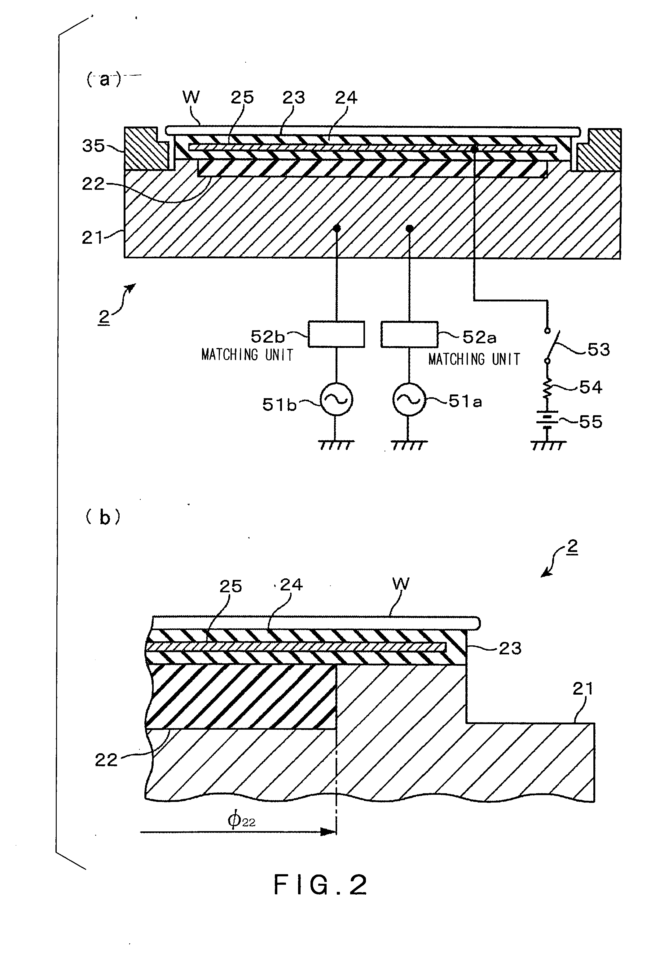
[0011] A table for use in a plasma processing system according to the present invention is a table for use in a plasma processing system, on which a substrate to be processed is placed, comprising an electrically conductive member connected to an RF (radio frequency) generator, functioning as an electrode for plasma formation or an electrode for attracting ions present in plasma; a first dielectric layer formed on the electrically conductive member so that it covers the center of the upper surface of the electrically conductive member, serving to make a high-frequency electric field to be applied to plasma via the substrate uniform; and a second dielectric layer having a relative dielectric constant of 100 or more, formed on the electrically conductive member so that it is in contact at least with the edge of the substrate, in order to prevent the high-frequency current that has propagated along the electrically conductive member face from leaking to the outside of the substrate and also to allow the high-frequency current to cause cavity cylindrical resonance of TM mode more efficiently.
[0017] In the table for use in a plasma processing system according to the present invention, a first dielectric is embedded in the center of the table so that cavity cylindrical resonance of TM mode occurs in it, thereby decreasing the field strength in this region to flatten the high field strength part of the field strength distribution in a mountain-like shape. Further, a second dielectric layer having a high relative dielectric constant, serving as a conducting path for a high-frequency current, is provided at least in the position corresponding to the edge of a substrate so that the high-frequency current is prevented from leaking from the edge of the substrate to the outside. Cavity cylindrical resonance of TM mode thus occurs more efficiently. Consequently, the electric potential in the center of the electric field to be applied to plasma from the substrate surface can be lowered, and the electric field within the substrate plane becomes uniform. There can thus be obtained a substrate processed in plasma processing, e.g., plasma etching, improved in within-substrate uniformity.
Problems solved by technology
Method used
View moreImage
Smart ImageViewing Examples

Examples
example 1
[0058] The relative dielectric constant ε24 of the upper dielectric layer 24 was set to 100.
example 2
[0059] The relative dielectric constant ε24 of the upper dielectric layer 24 was set to 900.
Login to View More PUM
 Abstract
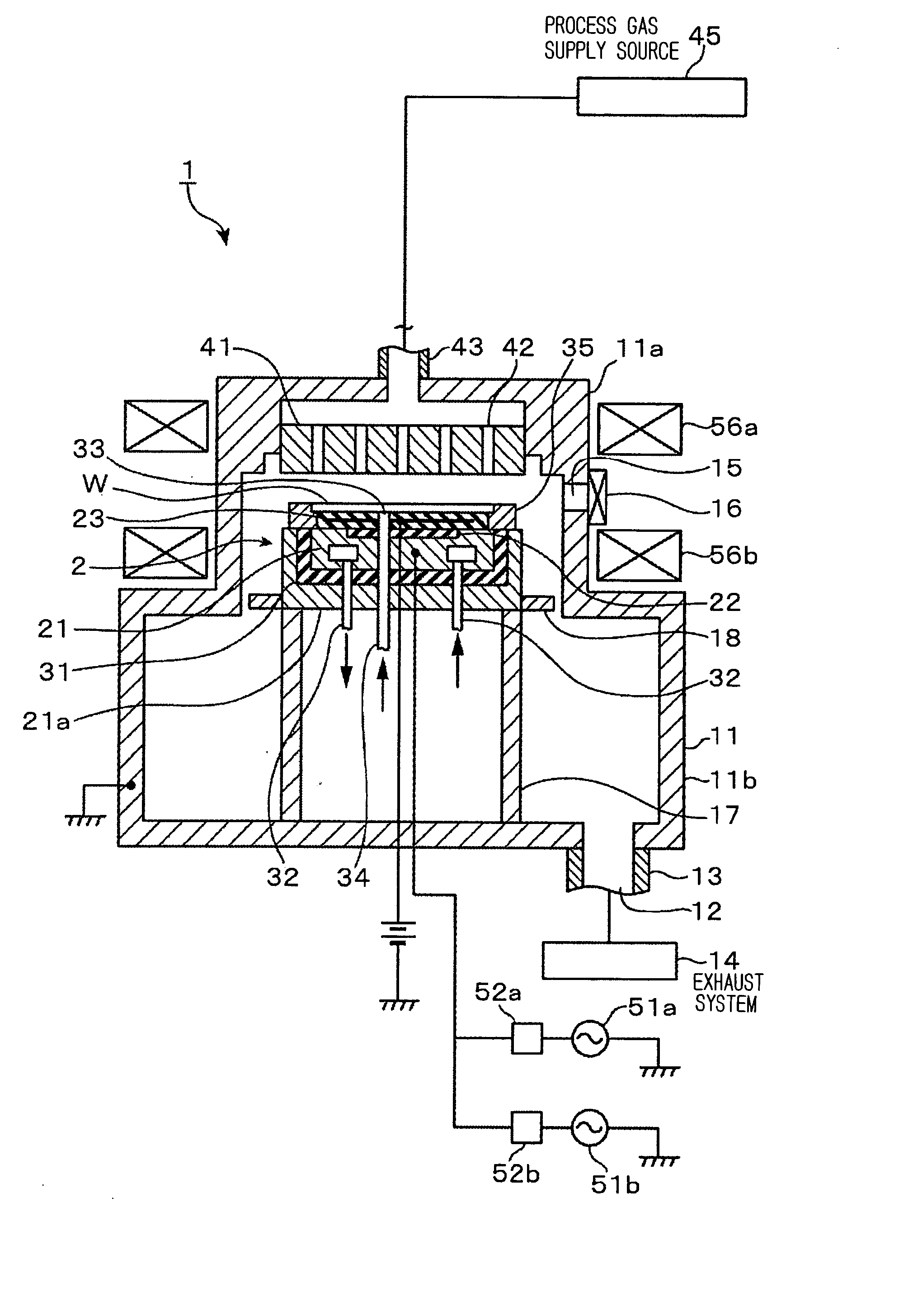
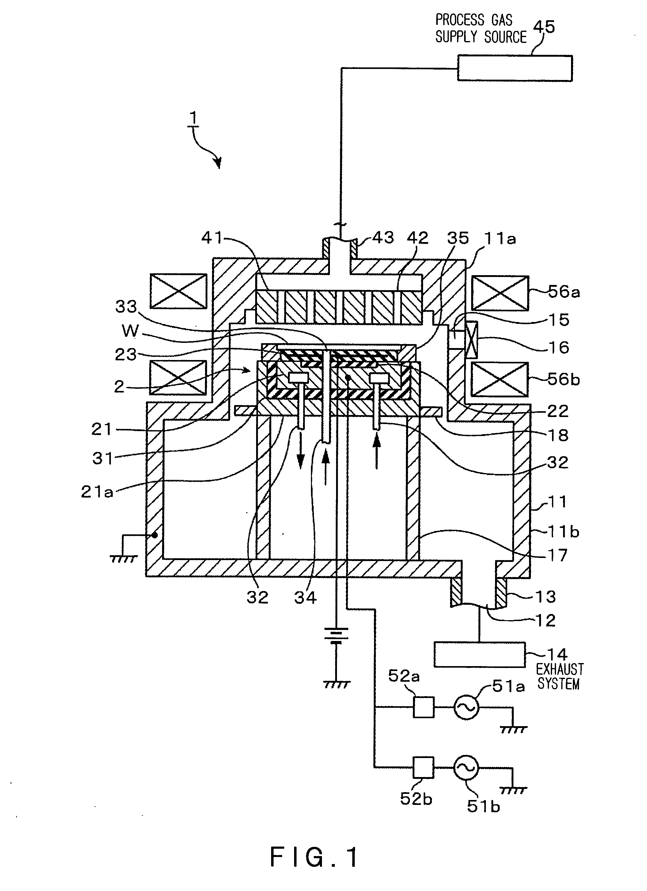
The present invention provides a table for use in a plasma processing system that makes it possible to obtain a substrate processed with plasma, improved in within-substrate uniformity, and a plasma processing system comprising such a table. A table 2 for use in a plasma processing system 1 comprises an electrically conductive member serving as a lower electrode 21 for plasma formation, a lower dielectric layer 22 (first dielectric layer) formed on the electrically conductive member so that it covers the center of the upper surface of the electrically conductive member, serving to make a high-frequency electric field to be applied to plasma via a substrate uniform, and an upper dielectric layer 24 (second dielectric layer) having a relative dielectric constant of 100 or more, formed on the electrically conductive member so that it is in contact at least with the edge of the substrate, in order to prevent a high-frequency current that has propagated along the electrically conductive member face from leaking to the outside of the substrate (wafer W).
Description
CROSS REFERENCE TO PRIOR APPLICATIONS [0001] This application claims priority from U.S. Provisional Application No. 60 / 844368 filed on Sep. 14, 2006, and Japanese Patent Application No. 2006-217873 filed on Aug. 10, 2006. The entire contents of these applications are incorporated herein by reference.BACKGROUND OF THE INVENTION [0002] 1. Field of the Invention [0003] The present invention relates to a table on which a substrate to be subjected to plasma processing, such as a semiconductor wafer, is placed, and to a plasma processing system comprising the table. [0004] 2. Background Art [0005] The process of semiconductor device production includes many processing steps in which a process gas is made into plasma and this plasma is used to process a substrate, such as dry etching and ashing. Of the plasma processing systems in which plasmas are used to process substrates, a processing system of the following type is often used: a pair of parallel plate electrodes are placed in a proces...
Claims
Login to View More Application Information
Patent Timeline
 IPC IPC(8): B01J19/08
CPCH01J37/32009H01J37/32532H01J37/32082
InventorKOSHIISHI, AKIRAHIMORI, SHINJIMATSUYAMA, SHOICHIRO
OwnerTOKYO ELECTRON LTD